Micro-electro-mechanical system chip and integrated circuit chip mixed packaging structure and packaging method thereof

A technology of micro-electromechanical chips and integrated circuits, which is applied in the direction of microstructure devices, manufacturing microstructure devices, and processing microstructure devices, etc., can solve the problems of low yield, low integration and difficult process, and achieve low cost and high integration. The effect of high and reduced dosage

Inactive Publication Date: 2018-01-05
黄卫东
View PDF10 Cites 2 Cited by
  • Summary
  • Abstract
  • Description
  • Claims
  • Application Information

AI Technical Summary

Problems solved by technology

[0010] The technical problem to be solved by the present invention is: to provide a hybrid packaging structure of micro-electromechanical chips and integrated circuit chips and its packaging method, which solves the problems of low integration of micro-electromechanical chips and integrated circuit chips, difficult process implementation, and good packaging in the prior art. low rate problem

Method used


Image

  • Micro-electro-mechanical system chip and integrated circuit chip mixed packaging structure and packaging method thereof
  • Micro-electro-mechanical system chip and integrated circuit chip mixed packaging structure and packaging method thereof
  • Micro-electro-mechanical system chip and integrated circuit chip mixed packaging structure and packaging method thereof

Examples


specific Embodiment 1

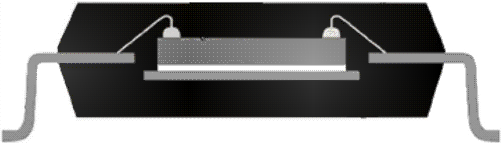
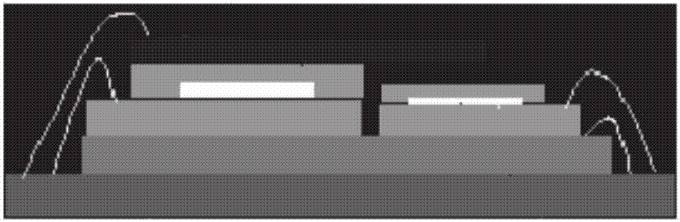
[0091] Such as Figure 5As shown, the hybrid packaging structure of micro-electromechanical chips and integrated circuit chips includes micro-electromechanical chips, integrated circuit chips, an upper substrate, a lower substrate, and a molding compound disposed between the upper substrate and the lower substrate. 4 integrated circuit chips, the 4 integrated circuit chips and the upper surface of the lower substrate are electrically connected through leads; a window is arranged on the upper substrate, and 3 micro-electromechanical chips are arranged in the window, and the connection between the 3 micro-electromechanical chips Electrical connections are formed between the upper substrate and the upper substrate through leads; epoxy solder flux filling materials are arranged between the upper substrate and the molding compound; electrical connections are realized between the upper substrate and the lower substrate through conductive through holes.

[0092] This embodiment only ...

specific Embodiment 2

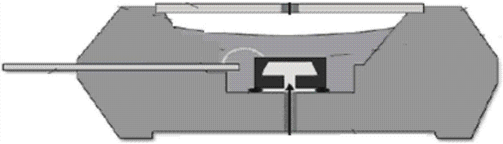
[0094] Such as Figure 6 As shown, the hybrid packaging structure of micro-electromechanical chips and integrated circuit chips includes micro-electromechanical chips, integrated circuit chips, an upper substrate, a lower substrate, and a molding compound disposed between the upper substrate and the lower substrate. 4 integrated circuit chips, the 4 integrated circuit chips and the upper surface of the lower substrate are electrically connected through leads; two windows are set on the upper substrate, one of which is equipped with 2 micro-electromechanical chips, and the other window A micro-electromechanical chip is arranged inside, and electrical connections are formed between the micro-electromechanical chips and the upper substrate through leads; epoxy flux filling material is arranged between the upper substrate and the molding compound; the upper substrate and the lower substrate are connected through conductive The through hole realizes the electrical connection.

[0...

specific Embodiment 3

[0097] Such as Figure 7 As shown, the hybrid packaging structure of micro-electromechanical chips and integrated circuit chips includes micro-electromechanical chips, integrated circuit chips, an upper substrate, a lower substrate, and a molding compound disposed between the upper substrate and the lower substrate. 4 integrated circuit chips, the 4 integrated circuit chips and the upper surface of the lower substrate are electrically connected through leads; two windows are set on the upper substrate, one of which is a sunken window, and 2 windows are set in the sunken window. One microelectromechanical chip, the other window is a raised window, and a microelectromechanical chip is arranged in the raised window, and electrical connections are formed between the microelectromechanical chips and the upper substrate through leads; the upper substrate and the molding compound are arranged Epoxy solder flux filling material; electrical connection between the upper substrate and th...


PUM


Abstract

The invention discloses a micro-electro-mechanical system chip and integrated circuit chip mixed packaging structure, comprising micro-electro-mechanical system chips, integrated circuit chips, an upper substrate, a lower substrate and plastic package glue arranged between the upper substrate and the lower substrate. The micro-electro-mechanical system chips, the integrated circuit chips and the upper substrate and / or the lower substrate are electrically connected. The upper substrate and the lower substrate are electrically connected. At least one window penetrating the upper substrate is arranged on the substrate. One or more micro-electro-mechanical system chips and / or integrated circuit chips are placed at the windows of the upper substrate, the surface of the lower substrate and / or the surface of the upper substrate. According to the scheme, the integration degree of the packaging structure is relatively high, the packaging integrated thickness is reduced through utilization of window structures, and the consumption of fillers is recued, so the cost is reduced. Pressure sensor chips may be integrated. The packaging structure has universality and is applicable to integrated packaging of various micro-electro-mechanical systems. A technology is easy to realize. The product quality is sufficiently ensured. The packaging yield calculated based on technology capability is higher than 99%.

Description

technical field [0001] The invention belongs to the field of chip packaging, and in particular relates to a hybrid packaging structure of a micro-electromechanical chip and an integrated circuit chip and a packaging method thereof. Background technique [0002] The integrated circuit (IC) chip is a new type of semiconductor device developed from the late 1950s to the 1960s. It is a semiconductor manufacturing process such as oxidation, photolithography, diffusion, epitaxy, aluminum evaporation, etc., which integrates transistors, resistors, capacitors and other components required to form a circuit with certain functions and the connecting wires between them into a small piece of silicon. On the surface of the silicon chip, then the circuit on the surface of the silicon chip is electrically connected to the outside and packaged. [0003] Integrated circuit packaging is the process of assembling integrated circuits into chip final products. It is to put the integrated circui...

Claims


Application Information

Patent Timeline
Patent Type & Authority Applications(China)
IPC IPC(8): B81B7/00B81B7/02B81C1/00B81C3/00H01L25/00
CPCH01L2924/10155H01L2224/48137H01L2224/48247H01L2224/73265
Inventor 黄卫东
Owner 黄卫东
Why Eureka
Try Eureka