Preparation method of amorphous transparent conductive oxide thin film

An oxide thin film, transparent and conductive technology, applied in ion implantation plating, metal material coating process, coating, etc., can solve the problems of severe carrier grain boundary scattering, process incompatibility, and large energy demand. Achieve less energy consumption, improve carrier mobility, reduce grain boundary scattering, ionized impurity scattering and carrier scattering

Inactive Publication Date: 2018-01-09
BEIJING JUNTAIINNOVATION TECH CO LTD
View PDF6 Cites 1 Cited by
  • Summary
  • Abstract
  • Description
  • Claims
  • Application Information

AI Technical Summary

Problems solved by technology

[0004] However, high-temperature annealing or high-temperature deposition requires a lot of energy, and is incompatible with some product processes. For example, the preparation process temperature of SHJ (silicon heterojunction) solar cells cannot be higher than 240 ° C, so the existing technology will also use room temperature Ho

Method used


Image

  • Preparation method of amorphous transparent conductive oxide thin film
  • Preparation method of amorphous transparent conductive oxide thin film
  • Preparation method of amorphous transparent conductive oxide thin film

Examples


Embodiment Construction

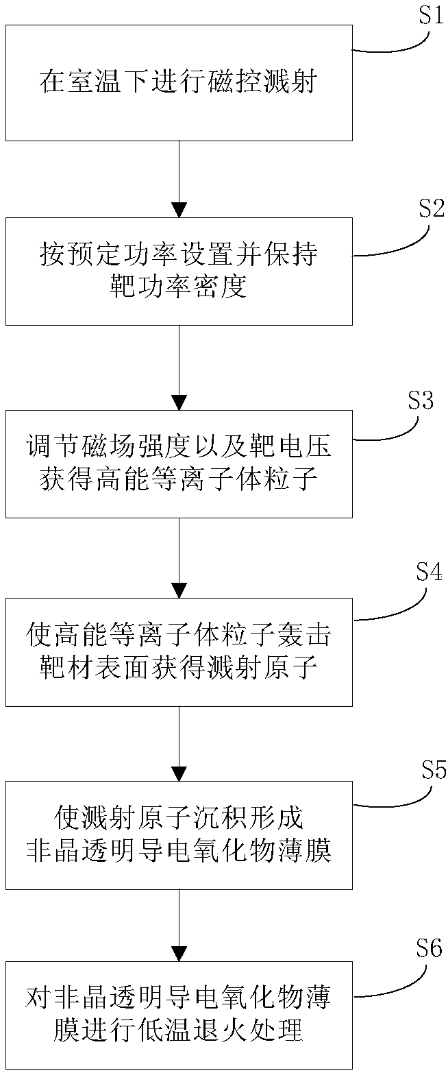
[0032] Embodiments of the present invention are described in detail below, examples of which are shown in the drawings, wherein the same or similar reference numerals designate the same or similar elements or elements having the same or similar functions throughout. The embodiments described below by referring to the figures are exemplary only for explaining the present invention and should not be construed as limiting the present invention.

[0033] Since the TCO film prepared under low temperature conditions in the prior art is a microcrystalline film, it is impossible to obtain a TCO film with a high mobility, and although high-temperature deposition and high-temperature annealing can obtain a TCO film with a high mobility, the resources required for it are More, the economic benefit is not good, accordingly the object of the present invention is to seek a kind of under low temperature condition, that is to say under the preparation condition that energy demand is not high, ...


PUM


Abstract

The invention discloses a preparation method of amorphous transparent conductive oxide thin film. The preparation method comprises the step of carrying out magnetron sputtering under the room temperature, and further comprises the steps of setting the target power density according to the preset power in the preparation process, and keeping the target power density unchanged; adjusting the magnetic field intensity and the target voltage to obtain the high-energy plasma particles with the energy higher than or equal to 100 eV; making the high-energy plasma particles bombard the surface of a target material to obtain sputtering atoms; making the sputtering atoms deposit on a base to obtain amorphous transparent conductive oxide thin film according to the preset deposition speed; and carryingout low-temperature annealing treatment on the amorphous transparent conductive oxide thin film. According to the preparation method of amorphous transparent conductive oxide thin film, grain boundary scattering, ionized impurity scattering and carrier scattering are greatly reduced, the influence caused by grain boundary scattering, ionized impurity scattering and carrier scattering to carrier mobility in amorphous transparent conductive oxide thin film obtained in the prior art is eliminated, and then, the purpose that the carrier mobility of TCO thin film is effectively improved on the premise that energy consumption is low is achieved.

Description

technical field [0001] The invention relates to the field of transparent conductive oxide films, in particular to a method for preparing an amorphous transparent conductive oxide film. Background technique [0002] Transparent conductive oxide (TCO) films have the dual advantages of transparency and conductivity, and are widely used in industries such as flat-panel displays, light-emitting diodes, and solar cells. TCO films with excellent performance must have high transmittance and lower resistivity. However, taking the application of solar cell industry as an example, the resistivity of TCO is directly proportional to the carrier concentration and carrier mobility, the carrier concentration decreases and the resistivity increases, resulting in a decrease in cell efficiency. Therefore, to improve the light transmittance of the TCO film while maintaining its good conductivity can only be achieved by increasing the mobility of the transparent conductive oxide film. Therefor...

Claims


Application Information

Patent Timeline
IPC IPC(8): C23C14/35C23C14/08C23C14/58
Inventor 何永才李建淸崔鸽董刚强郁操
Owner BEIJING JUNTAIINNOVATION TECH CO LTD
Why Eureka
Try Eureka