Self-circulation micro-fluidic chip as well as preparation method and usage of micro-fluidic chip

A microfluidic chip and chip technology, applied in chemical instruments and methods, laboratory containers, laboratory utensils, etc., can solve the problems of integrated safety, high working voltage, solution denaturation, etc., and achieve stability. Good, improve the output efficiency, the effect of the production method is simple

Active Publication Date: 2018-01-12
SHENZHEN GRADUATE SCHOOL TSINGHUA UNIV
View PDF3 Cites 20 Cited by
  • Summary
  • Abstract
  • Description
  • Claims
  • Application Information

AI Technical Summary

Problems solved by technology

Through a lot of research, there are few industrialized electroosmotic pumps on the market at present, and the early DC electroosmotic pumps will generate a lot of Joule heat due to their high working voltage, and the solution will also generate a lot of bubbles on the surface of the counter electrode. The electrode made of metal material will undergo electrolytic reaction with the solution, resulting in the consumption of the electrode and the denaturation of the solution, which has caused a series of problems for the integration of the microfluidic chip and the safety of the pump.

Method used


Image

  • Self-circulation micro-fluidic chip as well as preparation method and usage of micro-fluidic chip
  • Self-circulation micro-fluidic chip as well as preparation method and usage of micro-fluidic chip
  • Self-circulation micro-fluidic chip as well as preparation method and usage of micro-fluidic chip

Examples


Embodiment 1

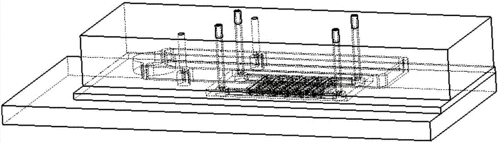
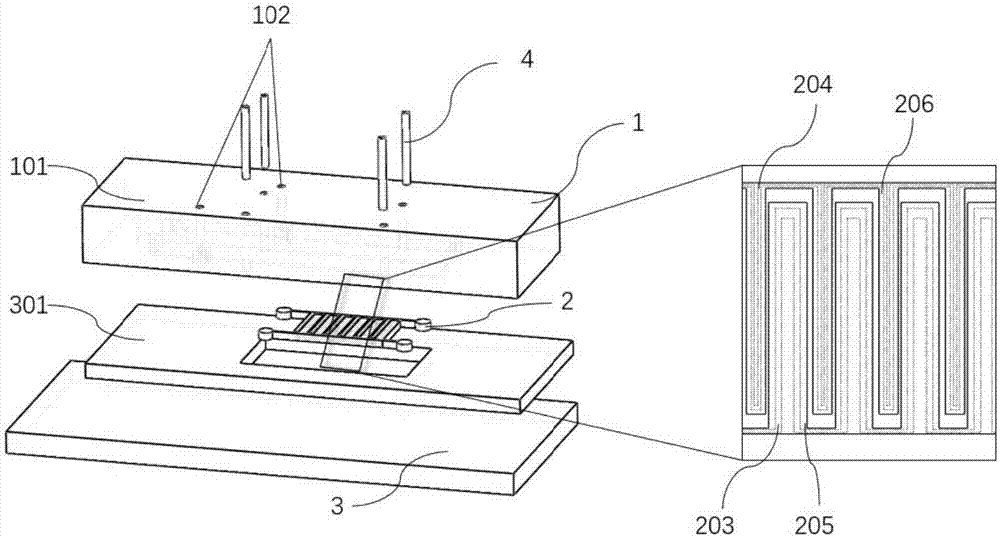
[0042] Such as figure 1 and figure 2 As shown, the self-circulating microfluidic chip of the present invention includes a top-down microfluidic layer 1 , an electroosmotic driving layer 2 and a chip substrate layer 3 . The electro-osmotic driving layer 2 and the microfluidic layer 1 and the chip base layer 3 respectively define mutually independent microfluidic flow channels and wide / narrow electrode liquid metal flow channels (203 / 204). The solution to be driven and the liquid metal are respectively perfused in the microfluid flow channel and the wide / narrow electrode liquid metal flow channel (203 / 204). Wherein the electroosmosis driving layer 2 and the wide / narrow electrode liquid metal flow channel (203 / 204) are interdigitated, and the lower surface of the electroosmotic driving layer 2 completely covers the wide / narrow electrode liquid metal flow channel ( 203 / 204), the upper surface of the electroosmotic driving layer 2 is exposed in the microfluidic channel. The two...

Embodiment 2

[0046] The preparation process of the microfluidic layer 1 is as follows: mix 20g of PMDS colloid and 2g of curing agent, rotate in a planetary mixer for 1min, then put the mixed PDMS liquid glue into a vacuum drying dish for 10min to vacuumize the prepared A good patterned silicon wafer is first placed in a Petri dish covered with aluminum foil to ensure that the silicon wafer is placed horizontally. Then put it into a light-proof glass dish, add 2 drops of trimethylchlorosilane solution, and take it out after fumigation for 2 minutes. The prepared PDMS liquid colloid was poured on a patterned silicon wafer, then placed in a vacuum drying dish to vacuum for 10 minutes, taken out and baked in an oven at 85°C for 30 minutes. Take out the cured PDMS and cut it according to the edge of the pattern. The plane size of the microfluidic layer 1 is 5cm×2cm. The entry regions 102 are each pierced with through holes with a diameter of 1 mm.

[0047] The preparation process of the elec...

Embodiment 3

[0053] Embodiment 3 is basically the same as Embodiment 2, except that the preparation process of the electroosmotic driving layer 2 is as follows:

[0054] Mix 20g of PDMS colloid with 100ml of chloroform and stir for 10min. 1.8 g of carboxylated multi-walled carbon nanotube powder and 1 g of porous carbon powder were mixed, ground in a mortar for 10 min, and poured into 100 ml of chloroform. Ultrasonic stirring was carried out in a 40 kHz ultrasonic cleaner for 1 h. After taking it out, mix the solution with the previously prepared PDMS / chloroform solution, and put it into a 40kHz ultrasonic cleaner for ultrasonic stirring for 2h. After taking it out, bake it on a heating plate at 80° C. for 8 hours until the solvent forms a colloidal state. Then put the prepared solution into a vacuum oven at 60° C. and bake for 2 hours. Apply the slurry on the aluminum foil, scrape it flat with a scraper, put it into a three-roll mill for rolling, and scrape the material off the aluminu...


PUM


Abstract

The invention discloses a self-circulation micro-fluidic chip, as well as a preparation method and a usage of the self-circulation micro-fluidic chip. The micro-fluidic chip comprises a microfluid layer, an electroosmosis driving layer and a chip base layer from top to bottom, wherein the electroosmosis driving layer defines a microfluid flow channel and a wide/narrow electrode liquid metal flow channel with the microfluid layer and the chip base layer respectively; the microfluid flow channel and the wide/narrow electrode liquid metal flow channel are independent and are filled with a to-be-driven solution and a liquid metal respectively; the electroosmosis driving layer and the wide/narrow electrode liquid metal flow channel are interdigital; the lower surface of the electroosmosis driving layer is completely covered with the wide/narrow electrode liquid metal flow channel; the upper surface of the electroosmosis driving layer is exposed in the microfluid flow channel; and the two ends of the wide/narrow electrode liquid metal flow channel are communicated with a power supply via four metal electrodes. The micro-fluidic chip has the advantages of small size, high integration level, portability, good stability and the like, is low in preparation cost and wide in application scope, and a preparation technology of the micro-fluidic chip is also very simple and practicable.

Description

technical field [0001] The invention belongs to the technical field of microfluid transport, and in particular relates to a self-circulating microfluidic chip and its preparation method and application. Background technique [0002] Microfluidic chips have been widely used in the biological field due to their small sample volume, high detection efficiency, and low cost of use. With the development of biological microfluidic chips in the direction of multifunctional integration, especially the demand for dynamic cultivation of biological cells, microfluidic chips must have chip self-driving functions without external equipment pump valves. However, most of the existing driving pumps require a huge external device source, which cannot realize the convenient portability of the chip, and the installation with the device source is relatively complicated. [0003] At present, it is more common to use a mechanical micropump to drive microfluidics, which has a relatively large driv...

Claims


Application Information

Patent Timeline
Patent Type & Authority Applications(China)
IPC IPC(8): B01L3/00
Inventor 弥胜利孙伟李柏翰李伟杜志昌王金杰
Owner SHENZHEN GRADUATE SCHOOL TSINGHUA UNIV
Why Eureka
Try Eureka