Reaction chamber and capacitive coupling plasma device

A reaction chamber and chamber technology, applied in the direction of circuits, discharge tubes, electrical components, etc., can solve the problems of etching by-products deposited on the inner side of the focus ring, affecting process stability, etc., to solve the problem of edge electric field effect, Improve the uniformity of etching and ensure the effect of the process

Pending Publication Date: 2018-01-12
BEIJING NAURA MICROELECTRONICS EQUIP CO LTD
View PDF0 Cites 13 Cited by
  • Summary
  • Abstract
  • Description
  • Claims
  • Application Information

AI Technical Summary

Problems solved by technology

[0006] In capacitively coupled plasma etching equipment, the edge electric field effect is very strong, and it is difficult to effectively solve the problem of excessive edge etching rate by increasing the height H of the focus ring and adjusting the inner diameter D of the focus ring; and, if the height H of the focus ring is too high Large, etch by-products are easy to deposit on the inner side of the focus ring, thus affecting the stability of the process

Method used


Image

  • Reaction chamber and capacitive coupling plasma device
  • Reaction chamber and capacitive coupling plasma device
  • Reaction chamber and capacitive coupling plasma device

Examples


Embodiment Construction

[0030] In order to make the purpose, technical solutions and advantages of the present disclosure clearer, the present disclosure will be further described in detail below in conjunction with specific embodiments and with reference to the accompanying drawings. It should be understood, however, that these descriptions are exemplary only, and are not intended to limit the scope of the present disclosure. Also, in the following description, descriptions of well-known structures and techniques are omitted to avoid unnecessarily obscuring the concepts of the present disclosure.

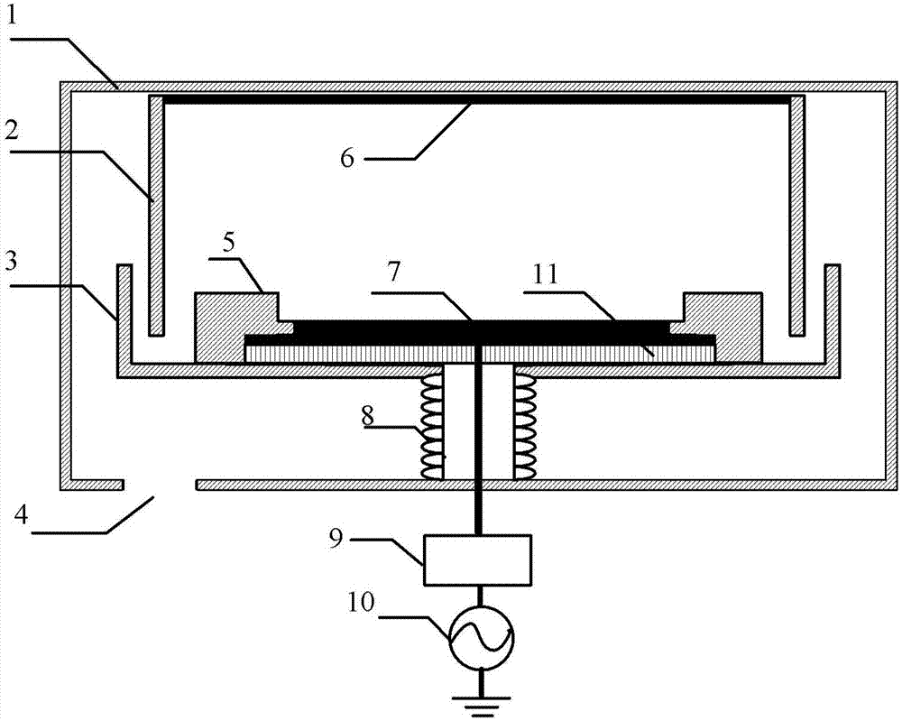
[0031] An embodiment of the present disclosure provides a reaction chamber, which is applied to capacitively coupled plasma equipment, especially capacitively coupled plasma pre-cleaning equipment, such as Figure 4 As shown, the reaction chamber is a cylindrical structure, including: a chamber body 1 , a lining and a lower electrode structure.

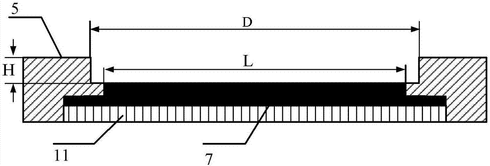
[0032] The chamber body 1 includes a side wall 11 and a bo...


PUM


Abstract

The invention provides a reaction chamber and a capacitive coupling plasma device. The reaction chamber comprises a bottom wall, a lining, a supporting assembly and a magnetic assembly. The lining isarranged in a chamber body and comprises a bottom lining located above the bottom wall of the chamber body. The supporting assembly is arranged in the process area surrounded by the bottom lining andused for supporting a wafer. The magnetic assembly is arranged outside the process area and used for forming a magnetic field so that the difference of the etching speeds of the edge area and the central area of the wafer can be reduced.

Description

technical field [0001] The present disclosure relates to the technical field of semiconductor manufacturing, and in particular to a reaction chamber and capacitively coupled plasma equipment. Background technique [0002] In the semiconductor etching process, the etching uniformity of the wafer is an important technical index. figure 1 It is a schematic diagram of the structure of a common capacitively coupled plasma (CCP) precleaning (Preclean) chamber. The chamber is generally a cylinder and consists of a chamber body 1, a lining (upper lining 2, lower lining 3), a lower electrode structure and other parts. The lower electrode structure is mainly composed of a support plate 7 , an insulating base 11 , a radio frequency matching device 9 and a radio frequency power supply 10 . The chamber body 1 is also provided with an exhaust port 4 through which reaction gases and etching by-products are exhausted. The gas uniform plate 6 makes the distribution of the gas entering the...

Claims


Application Information

Patent Timeline
Patent Type & Authority Applications(China)
IPC IPC(8): H01J37/32
CPCH01J37/32
Inventor 王文章陈鹏丁培军刘菲菲
Owner BEIJING NAURA MICROELECTRONICS EQUIP CO LTD
Why Eureka
Try Eureka