Eureka AIR delivers breakthrough ideas for toughest innovation challenges, trusted by R&D personnel around the world.

Microwave photonic broadband radar imaging chip and microwave photonic broadband radar imaging system

A broadband radar and microwave photon technology, applied in the field of microwave photon broadband radar imaging chips, can solve the problems of many control variables, high cost, complex system, etc., and achieve the effect of less control parameters, simple structure, and simple chip structure

Active Publication Date: 2018-01-16
NANJING UNIV OF AERONAUTICS & ASTRONAUTICS
View PDF5 Cites 19 Cited by
  • Summary
  • Abstract
  • Description
  • Claims
  • Application Information

AI Technical Summary

Problems solved by technology

In the above scheme, it is necessary to use an electronic 90° bridge to divide the electrical signal into two paths and load them into the two RF input ports of the DPMZM respectively. In order to generate positive and negative second-order sidebands, three DC bias voltages need to be applied to the DPMZM , in order to overcome the problem of bias voltage drift, it is necessary to configure a special bias control circuit. These factors lead to many control variables, complex system, and large volume
[0004] According to the above analysis, no matter what kind of photon-assisted technology is adopted, the existing microwave photon imaging radar solutions are all based on discrete optoelectronic devices, and the optoelectronic devices such as lasers, modulators, couplers, and detectors are connected by optical fibers, and have complex structures. , large volume, many control parameters, poor stability, high cost and other disadvantages

Method used


Image

  • Microwave photonic broadband radar imaging chip and microwave photonic broadband radar imaging system
  • Microwave photonic broadband radar imaging chip and microwave photonic broadband radar imaging system
  • Microwave photonic broadband radar imaging chip and microwave photonic broadband radar imaging system

Examples


Embodiment Construction

[0022] The technical scheme of the present invention is described in detail below in conjunction with accompanying drawing:

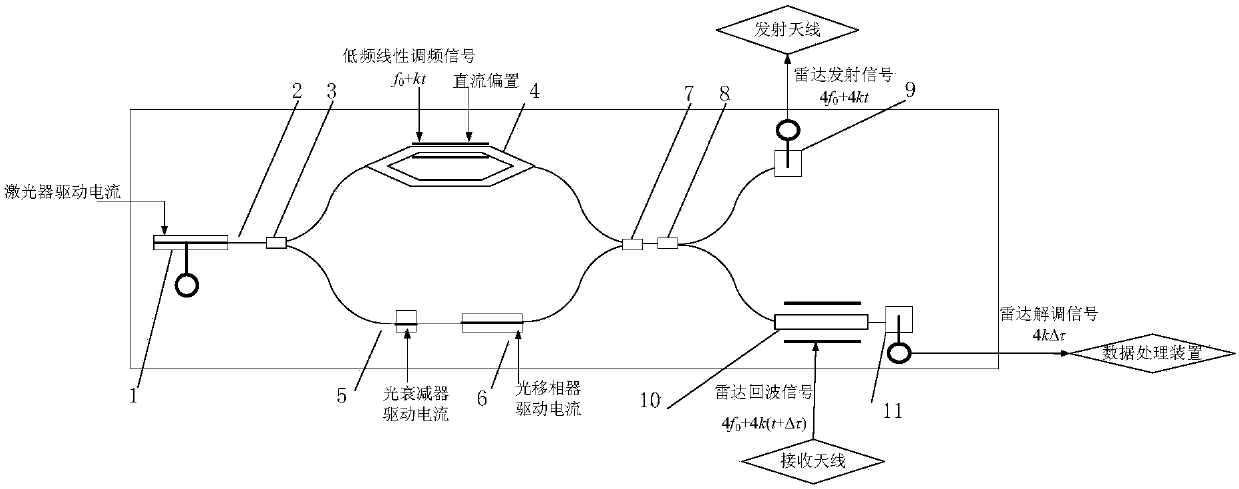
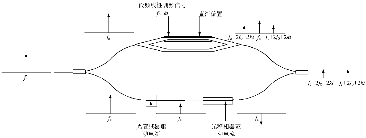
[0023] figure 1It is a schematic diagram of the structural principle of the microwave photon broadband radar imaging system proposed by the present invention, as shown in the figure, which includes: a transmitting antenna, a receiving antenna, a data processing device, and a microwave photon broadband radar imaging chip. The microwave photonic broadband radar imaging chip is integrated with the following photonic components: semiconductor laser 1, first 1×2 optical coupler 3, Mach-Zehnder modulator 4, optical attenuator 5, optical phase shifter 6, 2×1 Optical coupler 7, second 1×2 optical coupler 8, transmitting-end photodetector 9, phase modulator 10, receiving-end photodetector 11; each photon component is connected through optical waveguide 2; output end of semiconductor laser 1 Connect the input end of the first 1×2 optocoupler 3, the upper output ...


PUM


Abstract

The present invention discloses a microwave photonic broadband radar imaging chip, and belongs to the integrated microwave photonic technology field. According to the present invention, by a photonicIntegration technology, the emission end and the reception end of a microwave photonic broadband imaging radar are integrated in the same chip, the chip is integrated with the following photonic assemblies of a semiconductor laser, a first 1*2 optical coupler, a Mach-Zehnder modulator, an optical attenuator, an optical phase shifter, a 2*1 optical coupler, a second 1*2 optical coupler, an emissionend photoelectric detector, a phase modulator and a reception end photoelectric detector, and the photonic assemblies are connected via the optical waveguides. The present invention also discloses amicrowave photonic broadband radar imaging system. According to the present invention, a high-frequency broadband linear frequency modulation emission signal of the broadband imaging radar can be generated in the optical domain, and an echo can be demodulated to an intermediate frequency or a base band by utilizing a microwave photonic frequency mixing technology, so that the real-time processingof the high-resolution target imaging can be realized. The microwave photonic broadband radar imaging chip and the microwave photonic broadband radar imaging system of the present invention have theadvantages of being small in size, high in integration degree, good in stability and low in cost, etc.

Description

technical field [0001] The invention relates to a microwave photonic broadband radar imaging chip, which belongs to the technical field of integrated microwave photonics. Background technique [0002] In order to meet the needs of rapid and effective identification of dynamic targets in the fields of unmanned aerial vehicles, unmanned vehicles, and rapid security inspections, high-resolution real-time imaging radar systems have been deeply researched and explored. In order to realize high-resolution real-time imaging, it is required that the detection signal of the radar has a large bandwidth, and the echo signal can be processed quickly. At the radar signal transmitter, it is difficult to generate high-frequency and broadband chirp signals based on traditional electronic technology, which cannot meet the needs of high-resolution imaging. In order to overcome the shortcomings of electronic methods, the method of generating high-frequency broadband chirp signals based on pho...

Claims


Application Information

Patent Timeline
IPC IPC(8): G01S7/483G01S17/89
Inventor 李思敏潘时龙张方正
Owner NANJING UNIV OF AERONAUTICS & ASTRONAUTICS
Why Eureka
Eureka Blog
Learn More