Optical beam scanning chips integrated on VCSEL coupled array and optical phase shifter array sheet

A coupling array and beam scanning technology, which is applied in the direction of lasers, laser devices, laser components, etc., can solve the problems of complex installation process, complex overall structure, and difficult operation, and achieve the effects of small size, easy installation, and high reliability

Active Publication Date: 2018-01-19
BEIJING UNIV OF TECH
View PDF4 Cites 9 Cited by
  • Summary
  • Abstract
  • Description
  • Claims
  • Application Information

AI Technical Summary

Problems solved by technology

[0004] The purpose of the present invention is to solve the problems of complex overall structure, large volume, low reliability, complicated installation process and

Method used


Image

  • Optical beam scanning chips integrated on VCSEL coupled array and optical phase shifter array sheet
  • Optical beam scanning chips integrated on VCSEL coupled array and optical phase shifter array sheet
  • Optical beam scanning chips integrated on VCSEL coupled array and optical phase shifter array sheet

Examples


Embodiment

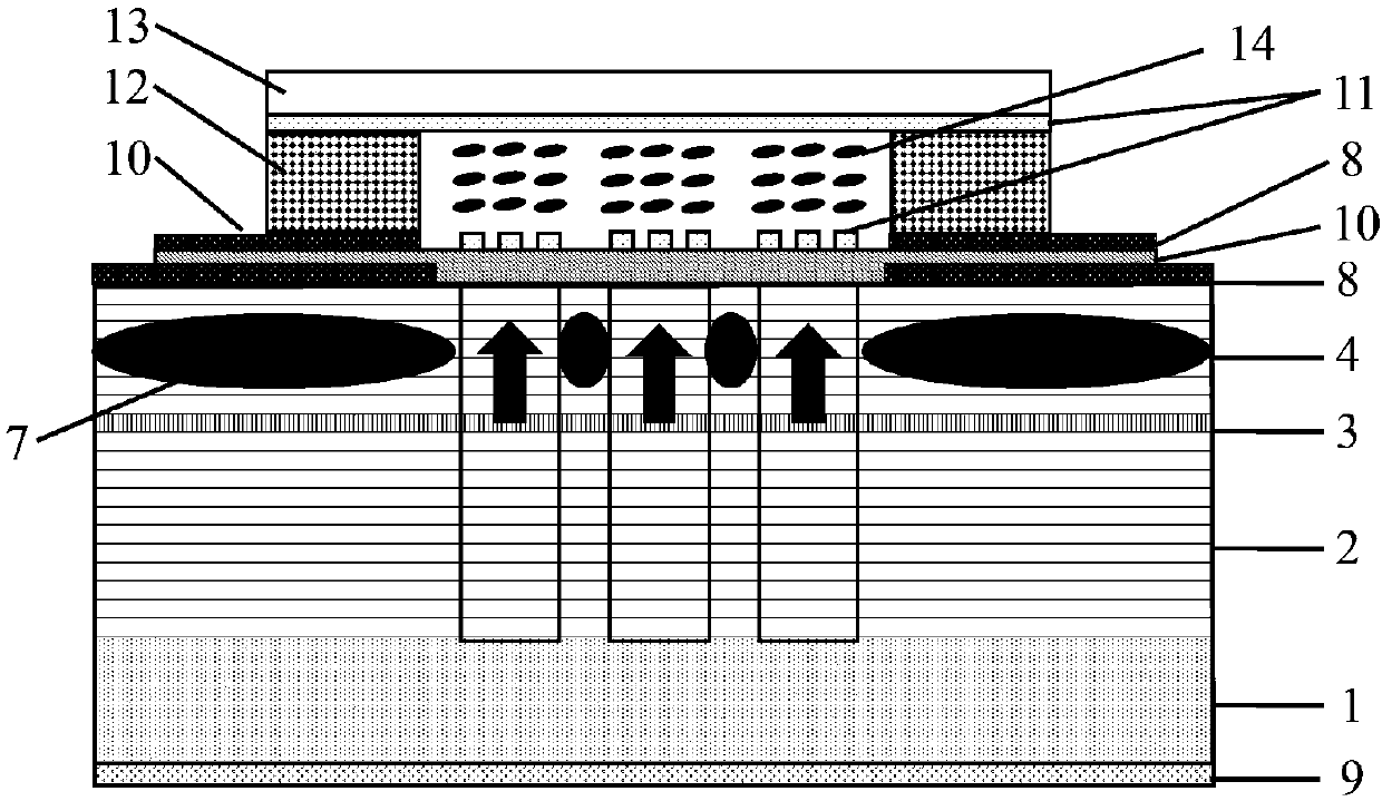
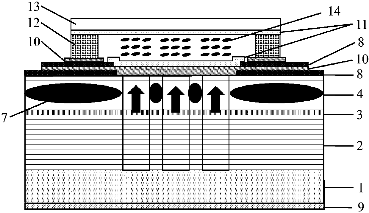
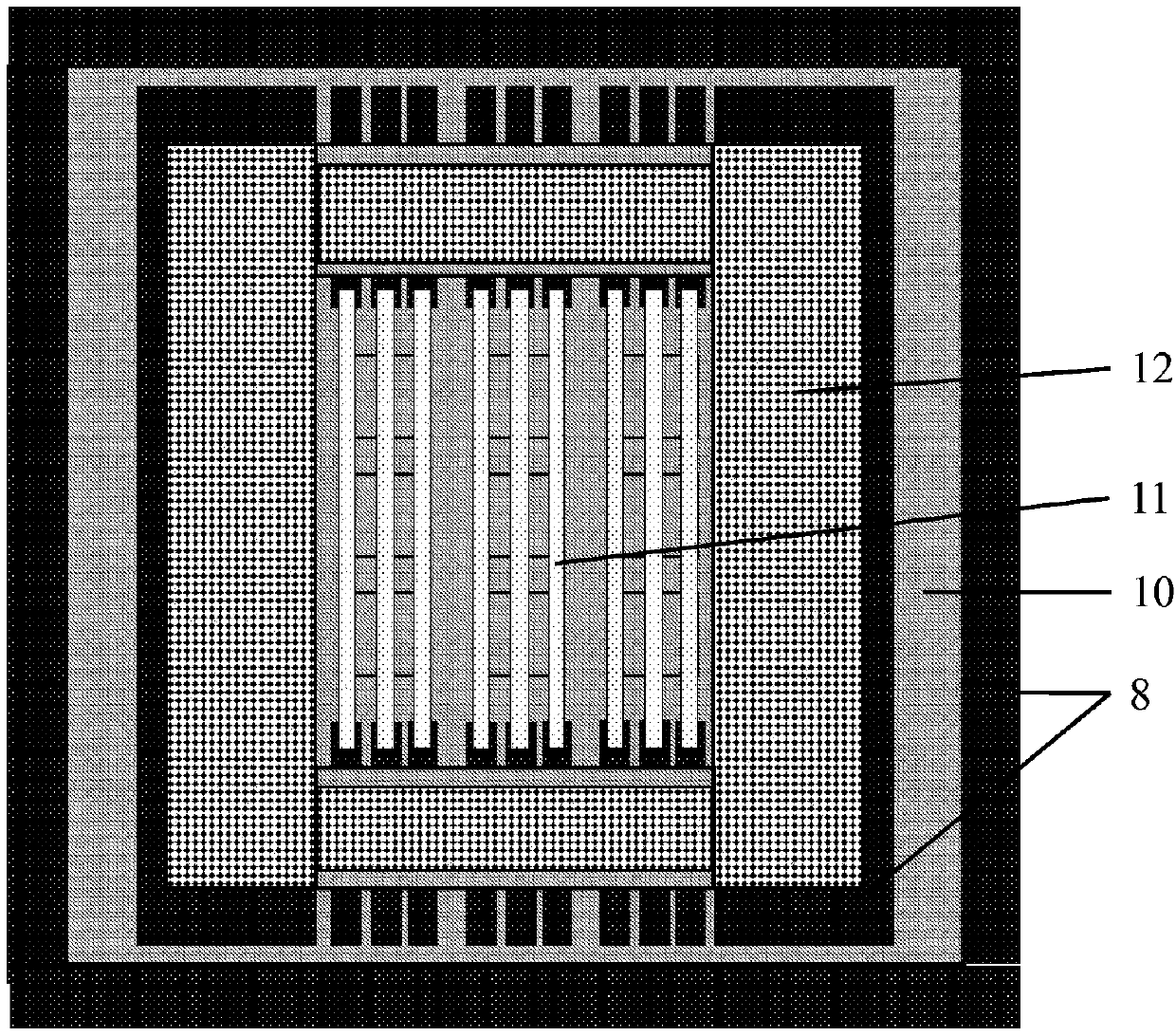
[0041] The present invention will be described in detail by taking the liquid crystal phase shifter array integrated on the surface of the proton injection type VCSEL coupling array as an example.

[0042] Combine below Figure 4-Figure 18 The specific implementation of the preparation method of the beam scanning chip integrated on the chip of the VCSEL coupling array and the optical phase shifter array is introduced respectively;

[0043] Step 1. Using metal-organic chemical vapor deposition (MOCVD) to sequentially epitaxially grow thirty-four pairs of n-Al on N-GaAs (0.12-0.9) GaAs and n-Al 0.9 GaAs forms the DBR mirror, Al (0.12-0.9) GaAs / Al 0.9 GaAs lower confinement layer, three pairs of Al 0.3 GaAs / GaAs quantum well structure active region, Al 0.9 GaAs / Al (0.12-0.9) GaAs upper confinement layer, 22.5 to p-Al 0.12 GaAs and p-Al (0.9-0.12) GaAs forms the DBR mirror, p-Al 0.12 GaAs and p-GaAs heavily doped contact layers;

[0044] Step 2, using plasma-enhanced che...


PUM

PropertyMeasurementUnit
Thicknessaaaaaaaaaa
Thicknessaaaaaaaaaa

Abstract

The invention discloses optical beam scanning chips integrated on VCSEL coupled array and a surface optical phase shifter array sheet, and belongs to the cross technical field of semi-conductor lasertechnologies and optical beam scanning technologies. A proton implantation technology, a photonic crystal or cavity induction reverse waveguide technology and the like are adopted, coupling among VCSEL array units is achieved, and coherent light with the same power can be generated by each array unit. By using characteristics of the VCSEL array plane structure, through technologies such as photolithography, sputtering, PECVD, ICP and evaporation, a transmissive optical phase shifter array is integrated on the surfaces of the VCSEL coupled array, and accordingly the optical beam scanning chipswith small size, compact structure and high integration level are obtained. The problems such as large size, low reliability and complex installation due to space separation of a laser source and thephase shifter array in a traditional optical phased array beam scanning device are solved, and the application prospects of the optical phase shifter sheet are wide.

Description

technical field [0001] The invention belongs to the intersecting technical field of semiconductor laser technology and beam scanning technology, and in particular relates to a beam scanning chip integrated on a chip of a VCSEL coupling array and an optical phase shifter array. Background technique [0002] Phased array optical technology is an optical technology that periodically modulates the optical phase of the beam wavefront. When each unit of the phase modulator array obtains a phase that is linearly distributed in space, the beam wavefront will be deflected in space. Generate a beam scan. This technology belongs to low-inertia purely electronically controlled non-mechanical beam scanning, which has scanning characteristics such as flexible beam pointing, fast scanning speed, high resolution, and large angular driving range. And other military and civilian fields have a wide range of applications and needs. The traditional optical phased array beam scanning device is ...

Claims


Application Information

Patent Timeline
IPC IPC(8): H01S5/183H01S5/40H01S5/00H01S5/34
Inventor 徐晨潘冠中解意洋王秋华董毅博
Owner BEIJING UNIV OF TECH
Why Eureka
Try Eureka