Multi-octave ultra-broadband amplifier circuit

An amplifier circuit, ultra-broadband technology, applied in the direction of amplifier combination, improved amplifier to expand bandwidth, electrical components, etc., can solve the problems of low unit circuit gain, power consumption and large chip area, so as to reduce the impact and realize high frequency Bandwidth, to achieve the effect of expansion

Inactive Publication Date: 2018-01-26
UNIV OF ELECTRONIC SCI & TECH OF CHINA
View PDF4 Cites 3 Cited by
  • Summary
  • Abstract
  • Description
  • Claims
  • Application Information

AI Technical Summary

Problems solved by technology

However, the amplifier with distributed structure has the disadvantages of low unit circuit gain, power consumption and large chip area.
Therefore, it is of great significance to carry out research on broadband amplifiers whose bandwidth is

Method used


Image

  • Multi-octave ultra-broadband amplifier circuit
  • Multi-octave ultra-broadband amplifier circuit
  • Multi-octave ultra-broadband amplifier circuit

Examples


Embodiment 1

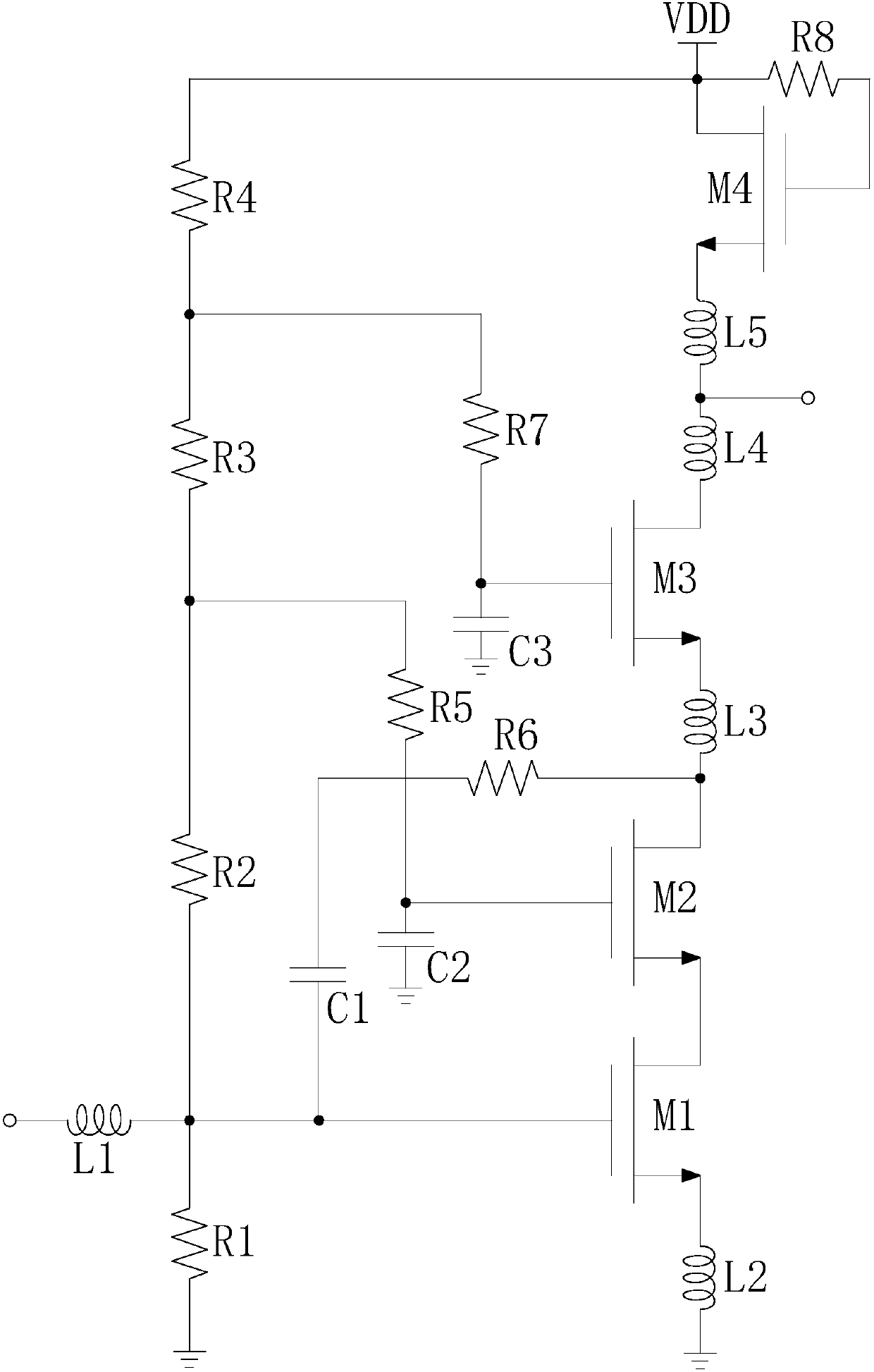
[0023] Such as figure 1 As shown, a multi-octave ultra-wideband amplifier circuit includes an input matching circuit, a cascode structure with three transistor stacks, a feedback circuit, a peaking inductor, an active-passive hybrid bias circuit, and a resistor Voltage divider network and power supply VDD, wherein, the transistors in the common source-common gate structure in this embodiment are any one of N-channel transistors, P-channel transistors, high electron mobility transistors and pseudo-high electron mobility transistors, figure 1 Shown is an N-channel transistor. The three transistors in the cascode structure of this embodiment are transistor M1, transistor M2, and transistor M3, the gate of transistor M1, the gate of transistor M2, the gate of transistor M3, and the active-passive hybrid bias The circuits are all connected to the power supply VDD, the source of the transistor M1 is grounded, as required by the cascode structure, the gate of the transistor M2 is gr...

Embodiment 2

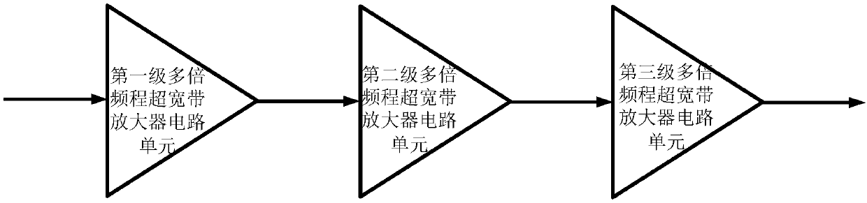
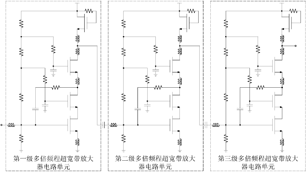
[0032] This embodiment makes the following further limitations on the basis of Embodiment 1: This embodiment cascades the amplifier circuit units in the three-stage implementation case 1 (the actual amplifier generally needs to be multi-stage cascaded to meet the requirements for gain, etc. The requirements of the index, each cascaded circuit is usually called an amplifier circuit unit), and its simulation results are given. figure 2 It is cascaded three levels figure 1 The circuit structure block diagram of the amplifier circuit shown includes a first-stage multi-octave UWB amplifier circuit unit, a second-stage multi-octave UWB amplifier circuit unit and a third-stage multi-octave UWB amplifier unit, image 3 yes figure 2 The block diagram shown corresponds to the circuit schematic. Such as image 3 As shown, the first-stage multi-octave UWB amplifier circuit unit, the second-stage multi-octave UWB amplifier circuit unit and the third-stage multi-octave UWB amplifier un...


PUM


Abstract

The invention discloses a multi-octave ultra-broadband amplifier circuit, which comprises a cascode structure stacked by three transistors, an active-passive hybrid bias circuit and a power supply VDD, wherein the three transistors in the cascode structure are a transistor M1, a transistor M2 and a transistor M3 respectively, wherein the grids of the transistor M1, the transistor M2 and the transistor M3 and the active-passive hybrid bias circuit are all connected to the power supply VDD; the source of the transistor M1 is connected to the ground; the grid of the transistor M2 is connected tothe ground through a capacitor C2; and the grid of the transistor M3 is connected to the ground through a capacitor C3. The source of the transistor M2 is connected to the drain of the transistor M1,the drain of the transistor M2 is connected to the source of the transistor M3, and the drain of the transistor M3 is connected to the active-passive hybrid bias circuit. According to the multi-octaveultra-broadband amplifier circuit, the working frequency covers megahertz (MHz) to gigahertz (GHz), the bandwidth is equivalent to a distributed amplifier, and the unit circuit gain performance, thepower consumption and the chip area are better than a distributed structure.

Description

technical field [0001] The invention relates to the technical field of wireless radio frequency communication, in particular to a multi-octave ultra-wideband amplifier circuit. Background technique [0002] In recent years, with the development of high-speed data transmission, optical fiber communication, broadband electromagnetic spectrum monitoring, software radio, cognitive radio system, etc., broadband transceivers have become more and more widely used. Traditional broadband transceivers use multiple receivers covering different frequency bands to connect in parallel to achieve broadband coverage. Due to the use of receivers in different frequency bands, there will be multiple blocks of the same type of general-purpose modules (such as low-noise amplifiers, power amplifiers, etc.). This leads to a substantial increase in the size, cost, and power consumption of the device, and a significant reduction in reliability, which limits the popularization and application of broa...

Claims


Application Information

Patent Timeline
IPC IPC(8): H03F1/42H03F3/68H04B1/40
Inventor 马凯学胡建全
Owner UNIV OF ELECTRONIC SCI & TECH OF CHINA
Why Eureka
Try Eureka