ESD full-shielding functional foil, ESD full-shielding functional foil circuit board and manufacturing methods

A fully shielded and circuit board technology, which is applied to printed circuit components, magnetic field/electric field shielding, electrical components, etc., can solve the problems of no precise positioning requirements, increased production costs, and inability to do what one wants

Pending Publication Date: 2018-01-26
WUHAN CHIP PROTECTION TECH
View PDF16 Cites 3 Cited by
  • Summary
  • Abstract
  • Description
  • Claims
  • Application Information

AI Technical Summary

Problems solved by technology

Also because of manufacturing cost considerations, it is impossible to provide comprehensive protection for all pins of all sensitive devices in the circuit
[0004] Chinese patent ZL201220475284.6 "A Printed Circuit Board with All-round Antistatic Function" adopts the method of surface-mounted polymer composite nano-varistor soft film, which can completely solve the problem of single-layer circuit board or double-sided board and low-density small The electronic circuits of large-scale wiring equipment can resist the impact of instantaneous high-voltage electric pulse energy, but for large-scale, high-density wiring electronic circuits and multilayer circuit boards, this solution is obviously powerless
When using this solution to produce circuit boards, due to the limited thickness requirements of the new standard for circuit boards in reality (for example, the thickness of circuit boards such as mobile phones has dropped from the original 1.20mm to the current 0.7mm±0.08mm), this gives the "functional core board The application of " brings limitations:
[0008] ②At present, the drilling accuracy error is 5%, and it is impossible to achieve an accuracy of 0.005mm within this error range
[0009] ③If there is a problem with a hole in a circuit board during production, the entire circuit board will be scrapped, so the product qualification rate brought by this manufacturing method must be extremely low
Three years ago, the thickness requirement of circuit boards such as mobile phones was still 1.2mm, and the current thickness standard is 0.7mm, which makes the thickness of the small metal squares in this technology have to be reduced from greater than 0.1mm to less than 0.05mm. This technique brings with it great difficulties
A mobile phone board has hundreds or thousands of attached copper wires. If they are all protected, hundreds of thousands of via holes must be made at the same time, which will make the process more complicated. This will also increase the production cost and lose the meaning of the invention.
[0013] ②Since the via hole is on the ground layer in the PCB interlayer, it needs to be pre-processed. After the via hole is embedded in the PCB board, it cannot be seen. The selection of the drilling position must be absolutely accurate. The original patent design error can be one to one There is no precise positioning requirement for the range of motion of the four small squares, but after the vias are provided, the positions of the vias must be absolutely aligned, even if the deviation is only 0.01mm, it will cause a short circuit between the via hole and the metal block, and the PCB board will be scrapped

Method used


Image

  • ESD full-shielding functional foil, ESD full-shielding functional foil circuit board and manufacturing methods
  • ESD full-shielding functional foil, ESD full-shielding functional foil circuit board and manufacturing methods
  • ESD full-shielding functional foil, ESD full-shielding functional foil circuit board and manufacturing methods

Examples


Embodiment Construction

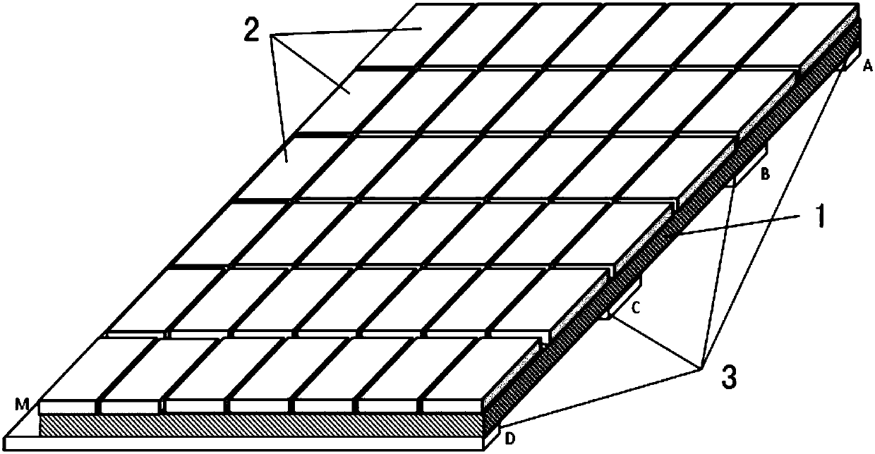
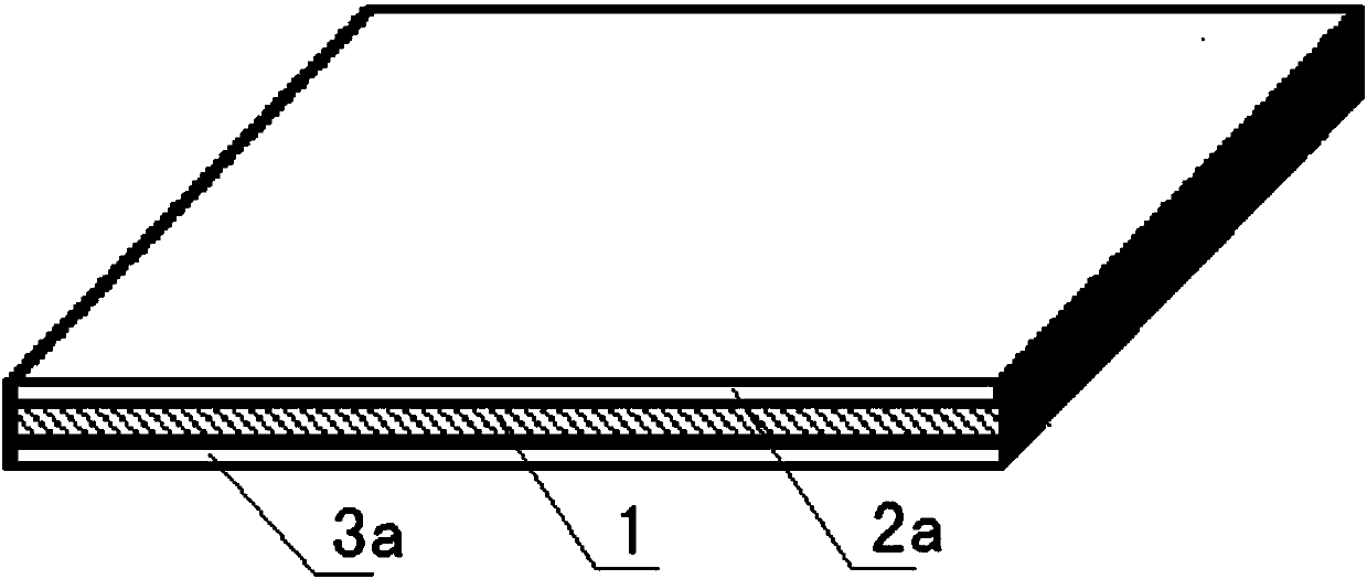
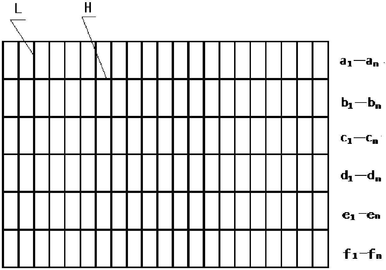
[0061] Such as figure 1 , figure 2 , image 3 , Figure 4 , Figure 5 :

[0062]An ESD full-shielding functional foil of the present invention includes a basic functional foil, the basic functional foil has a layer of functional material layer 1 and a metal layer attached to the upper and lower surfaces of the functional material layer 1, and the upper metal layer of the functional material layer 1 is etched with multiple lines, Multiple columns of strip-shaped metal blocks form a strip-shaped metal block array. Between the rows and columns of the strip-shaped metal block array are longitudinal spacers L and horizontal spacers H. The strip-shaped metal blocks arranged at regular intervals form a strip-shaped metal block array layer 2; The lower metal layer is etched into a metal ground wire for grounding, and the metal ground wire is composed of parallel and equally spaced ground wires A, B, C, D... and M wires connecting A, B, C, D..., equally spaced The ground wires A,...


PUM

PropertyMeasurementUnit
thicknessaaaaaaaaaa
thicknessaaaaaaaaaa

Abstract

The invention provides an ESD full-shielding functional foil, an ESD full-shielding functional foil circuit board and manufacturing methods. The core is the ESD full-shielding functional foil; the ESDfull-shielding functional foil comprises a functional material layer; multiple rows and multiple columns of bar metal blocks are etched on an upper metal layer of the functional material layer to form a bar metal block array layer; a lower metal layer is etched into a metal ground wire for grounding; the metal ground wire comprises parallel uniformly-spaced ground wires A, B, C, D ... and a lineM connecting the ground wires A, B, C, D ...; the uniformly-spaced ground wires A, B, C, D ... are located on transverse spacers of a bar metal block array, each uniformly-spaced ground wire overlapswith one end of the corresponding bar metal block, each row of bar metal blocks overlap with the corresponding ground wire, and electrostatic pulse absorption tunnels are formed at the overlapping parts. An instantaneous electric energy release network is built by putting the ESD full-shielding functional foil into any interlayer of a PCB, so that components on the circuit board generate a shielding effect on instantaneous high-voltage electric pulse energy.

Description

technical field [0001] The invention relates to an ESD full-shielding functional foil, an ESD full-shielding functional foil circuit board and a manufacturing method, belonging to the technical field of electronic manufacturing, and providing a brand-new ESD full-shielding functional product for PCB board manufacturing of electronic products. Background technique [0002] The present invention is based on the technical invention of the Chinese patent ZL201410195406.X "a circuit board core board capable of absorbing instantaneous high voltage and its manufacturing method". A special functional foil is provided for the purpose of solving the specific problems that are difficult to overcome in the processing technology. [0003] In the circuit of electronic equipment, in order to prevent the impact of transient high-voltage pulse energy, such as static electricity, surge and transient electric potential field induction energy, most of them are equipped with absorption circuits ...

Claims


Application Information

Patent Timeline
Patent Type & Authority Applications(China)
IPC IPC(8): H05K9/00H05K1/02
Inventor 龚德权王晶
Owner WUHAN CHIP PROTECTION TECH
Why Eureka
Try Eureka