
Multi-chip stacked package structure and packaging method thereof

A technology of packaging structure and packaging method, which is applied in the direction of semiconductor/solid-state device parts, semiconductor devices, electrical components, etc., can solve the problems of large volume, increased resistance and thermal resistance, and affect the performance of finished devices, so as to achieve good performance and good electrical conductivity. The effect of reducing loss and switching loss and saving packaging materials

Active Publication Date: 2018-02-09
ALPHA & OMEGA SEMICON INT LP
View PDF4 Cites 2 Cited by
  • Summary
  • Abstract
  • Description
  • Claims
  • Application Information

AI Technical Summary

Problems solved by technology

However, for a specific packaging structure, the above-mentioned high-end MOSFET chip, low-end MOSFET chip and controller chip can only be arranged in parallel on the same plane of the lead frame, so the volume after packaging is large; moreover, they are only connected by wires The corresponding pins of the chip (for example, between the source S1 of the HS and the drain D2 of the LS) will increase the resistance and thermal resistance, which will affect the performance of the finished device

Method used


Image

  • Multi-chip stacked package structure and packaging method thereof
  • Multi-chip stacked package structure and packaging method thereof
  • Multi-chip stacked package structure and packaging method thereof

Examples


Embodiment 1

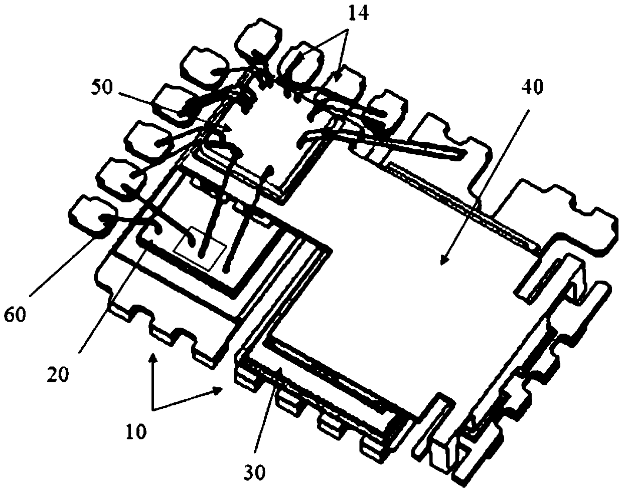
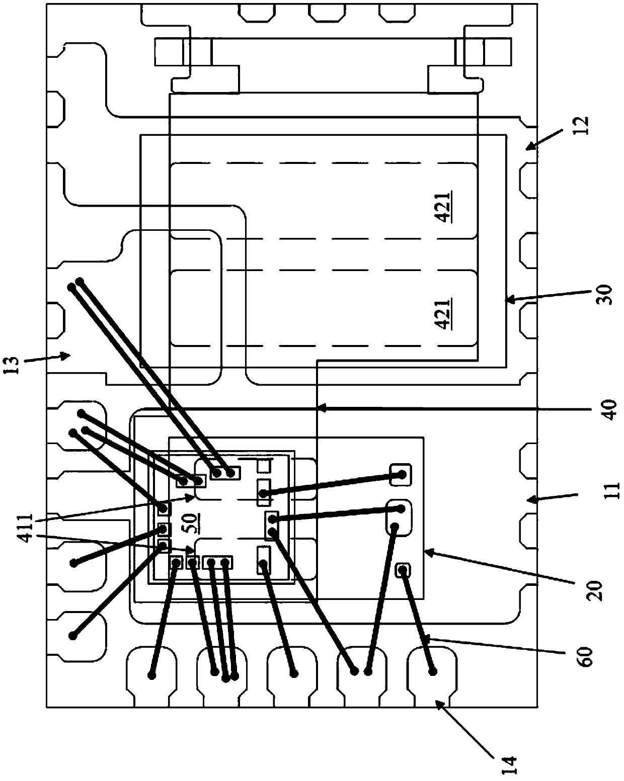
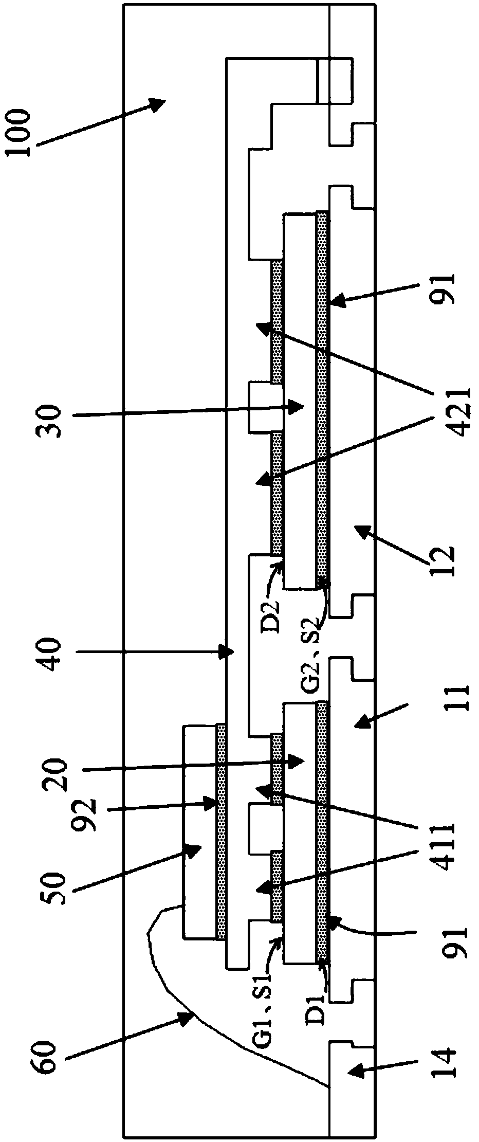
[0071] Cooperate see Figure 1A ~ Figure 1C As shown, in the present invention, by 2 MOSFET chips of the same type (2 N-type or 2 P-type), respectively as high-end MOSFET (abbreviated as HS chip 20) and low-end MOSFET chip (abbreviated as LS chip 30). A controller chip (abbreviated as IC chip 50) is stacked on the same plane where the two MOSFET chips are located by a bonding sheet 40, and the IC chip 50 is connected to the corresponding electrodes and electrodes of the LS chip 30 and the HS chip 20. After the pins 14 are connected, they are packaged in the same plastic package 100 to form a DC-DC converter.

[0072] The HS chip 20 and the LS chip 30 are respectively provided with a source and a gate on the front of the chip, and a drain is provided on the back of the chip; wherein, the gate G1 of the HS chip 20 and the gate G2 of the LS chip 30 are both It is connected with the control pole on the IC chip 50; the drain D1 of the HS chip 20 is connected to the Vin end, the so...

Embodiment 2

[0098] Figure 4A ~ Figure 4G It shows the schematic structure in each step of chip packaging in this embodiment, Figure 5 The flow of the encapsulation method in this embodiment is shown. Wherein, the structure of the present embodiment is briefly described as follows, that is, a lead frame 10 ( Figure 4A ), including the first loading stage 11, which is used to fixedly connect the HS chip 20 and form an electrical connection with its backside drain D1 ( Figure 4B ); It also includes a second loading table, which is provided with a first part 12 and a second part 13, which are used to fix and connect the flipped package LS chip 30 and form an electrical connection with the source S2 and the grid G2 on the front side respectively ( Figure 4C ). A connecting piece 40 is conductively connected on the HS chip 20 and the LS chip 30, so that the high-side connection portion 41 of the connecting piece 40 is electrically connected to the source S1 on the front side of the HS ...

Embodiment 3

[0102] Figure 6A ~ Figure 6G It shows the schematic structure in each step of chip packaging in this embodiment, Figure 7The flow of the encapsulation method in this embodiment is shown. Wherein, the structure of the present embodiment is briefly described as follows, that is, a lead frame 10 ( Figure 6A ), including the first loading stage 11, which is used to fixedly connect the HS chip 20 and form an electrical connection with its backside drain D1 ( Figure 6B ); It also includes a second loading table, which is provided with a first part 12 and a second part 13, which are used to fix and connect the flipped package LS chip 30 and form an electrical connection with the source S2 and the grid G2 on the front side respectively ( Figure 6C ). A connecting piece 40 is conductively connected on the HS chip 20 and the LS chip 30, so that the high-side connection portion 41 of the connecting piece 40 is electrically connected to the source S1 on the front side of the HS ch...


PUM


Abstract

The present invention relates to a multi-chip stacked package structure and a packaging method thereof. According to the multi-chip stacked package structure and the packaging method thereof, only oneconnection sheet is disposed on the source of an HS chip and the drain of an LS chip to achieve the electrical connection of the HS chip and the LS chip, the conduction loss and switching loss of thepackage structure are reduced, and the heat dissipation efficiency of the package structure is enhanced; an IC chip is connected with the connection sheet in an insulated manner, and therefore, the IC chip can be stacked above a plane where the HS chip and the LS chip are located, and therefore, the size of a packaged device can be effectively decreased; the bottom surfaces of a first chip carrying stage and a second chip carrying stage can be exposed outside a package body; optionally, a part of the surface of a portion of the connection sheet which is not connected with the IC chip is exposed outside the package body; optionally, a heat dissipation plate is connected onto the connection sheet, and a part of the surface of the heat dissipation plate is exposed outside the package body; and optionally, the heat dissipation plate is inserted into a gap reserved in the package body so as to contact with the connection sheet to facilitate heat dissipation.

Description

[0001] This case is a divisional application [0002] Title of the original invention: A multi-chip stacked packaging structure and its packaging method [0003] Original application number: 201310617032.1 [0004] Date of original filing: November 27, 2013 technical field [0005] The invention relates to the field of semiconductors, in particular to a multi-chip stacked package structure and a package method thereof. Background technique [0006] In a DC-DC (direct current-direct current) converter, there are usually two MOSFETs (metal oxide semiconductor field effect transistors) as switching switches, one is a high-side MOSFET (HS for short), and the other is a low-side MOSFET (LS for short). ). Among them, the gate G1 of HS and the gate G2 of LS are connected to a controller (abbreviated as IC); the drain D1 of HS is connected to the Vin terminal, the source S1 is connected to the drain D2 of LS, and the source S2 of LS is connected to Gnd terminal to form the DC-DC...

Claims


Application Information

Patent Timeline
Patent Type & Authority Applications(China)
IPC IPC(8): H01L23/495H01L25/16H01L23/31H01L23/367H01L21/98
CPCH01L23/3672H01L23/4922H01L23/49562H01L23/49568H01L24/84H01L25/072H01L23/3107H01L23/49531H01L23/49575H01L25/16H01L25/50H01L2924/181H01L2224/0603H01L2224/05554H01L2224/05553H01L2224/48137H01L2224/48247H01L2224/32245H01L2224/37H01L2224/37147H01L2224/40137H01L2224/40139H01L2224/40095H01L2224/40H01L2224/40245H01L2224/73265H01L2224/49111H01L2224/8385H01L2224/84986H01L2224/8485H01L2924/13091H01L2924/13055H01L2924/00H01L2924/00012H01L24/40H01L24/37H01L24/48H01L2224/84345H01L2224/73221H01L2924/00014
Inventor 张晓天潘华鲁明朕鲁军哈姆扎·依玛兹
Owner ALPHA & OMEGA SEMICON INT LP
Learn More