

Organic light emitting display (OLED) panel and fabrication method thereof
A manufacturing method and panel technology, applied in semiconductor/solid-state device manufacturing, diodes, semiconductor devices, etc., can solve the problems affecting the aperture ratio and small storage capacitor capacity, so as to increase the aperture ratio, increase the storage capacitor, and reduce the design area Effect
- Summary
- Abstract
- Description
- Claims
- Application Information
AI Technical Summary
Problems solved by technology
Method used
Image


Examples
Embodiment Construction
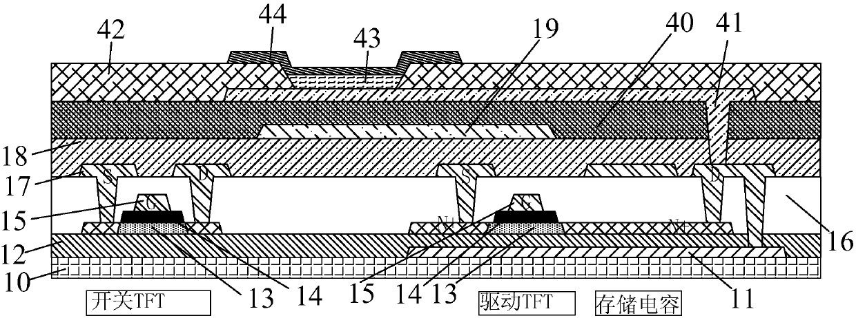
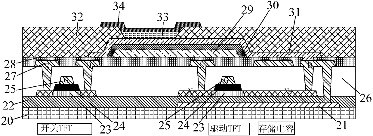
[0032] see figure 2 , which is a structural diagram of a preferred embodiment of the OLED panel of the present invention, which can be divided into a switching TFT area, a driving TFT area, and a storage capacitor area according to functional areas. The OLED panel of the present invention mainly includes: a glass substrate 20; a TFT light-shielding layer 21 fabricated on the glass substrate 20; a buffer layer 22 deposited on the TFT light-shielding layer 21; a semiconductor layer 23 deposited on the buffer layer 22, and a semiconductor layer 23 Patterned as the TFT active layer; the gate insulating layer 24 and the first metal layer 25 deposited on the semiconductor layer 23, the gate insulating layer 24 and the first metal layer 25 are patterned to form the gate of the TFT , and the semiconductor layer 23 outside the area covered by the first metal layer 25 is subjected to conducting treatment, such as increasing the doping concentration in the area where the semiconductor l...
PUM
 Abstract
Description
Claims
Application Information