Measurement method of device surface state traps based on variable frequency pulse technique

A pulse technology and device surface technology, applied in the field of microelectronic device testing, can solve the problems of reduced device output power, lack of in-depth analysis of surface state physical characteristics, and inability to obtain trap response conditions, achieving simple testing methods and mature process technology. stable effect

Active Publication Date: 2019-02-22
XIDIAN UNIV
View PDF9 Cites 0 Cited by
  • Summary
  • Abstract
  • Description
  • Claims
  • Application Information

AI Technical Summary

Problems solved by technology

As the most mature and convincing theory in the formation mechanism of the current collapse effect, the virtual gate model believes that when the device is working at a high voltage, a large number of electrons tunnel through the gate metal, and these electrons are captured by the surface state traps of the device. The electrostatic suppression of the two-dimensional electron gas leads to the reduction of the output power of the device
[0004] The traditional method of measuring the current collapse of a device is to perform a pulse voltage test on the device. Since the time constants of these surface state traps capture or release electrons are different, the responses under pulse voltages of different pulse widths are different. By comparing different pulse voltages and DC The maximum output current under the voltage can be used to obtain the current collapse. However, this test method cannot obtain the response of the trap under different pulse voltages, and there is still a lack of in-depth analysis of the physical characteristics of the surface state.

Method used


Image

  • Measurement method of device surface state traps based on variable frequency pulse technique
  • Measurement method of device surface state traps based on variable frequency pulse technique
  • Measurement method of device surface state traps based on variable frequency pulse technique

Examples


Embodiment Construction

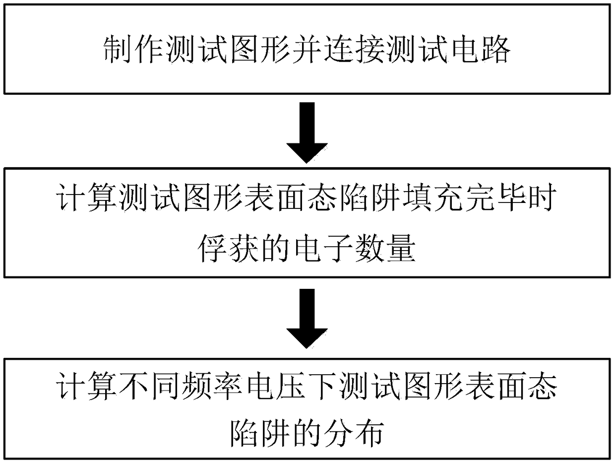
[0036] The specific implementation of the present invention will be further described in detail below in conjunction with the accompanying drawings and examples. The examples are used to illustrate the present invention, but not to limit the scope of the present invention.

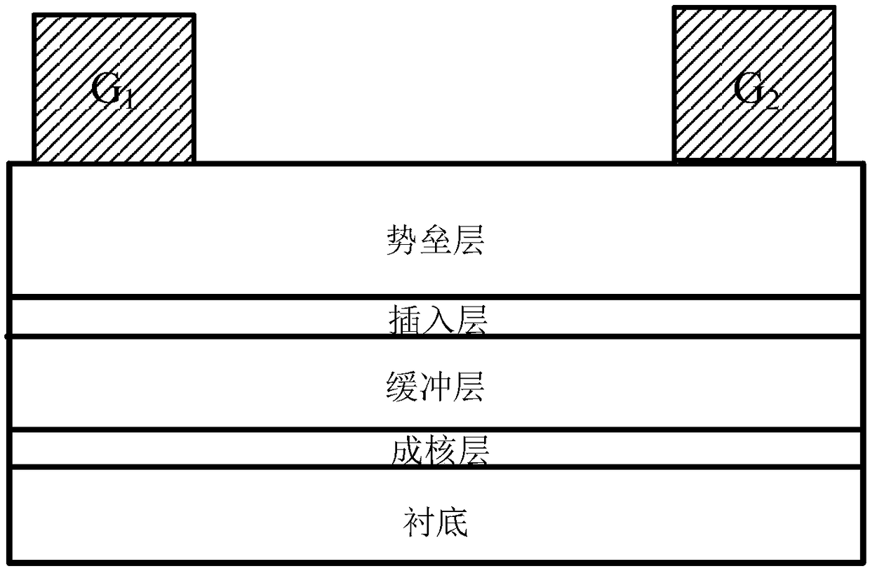
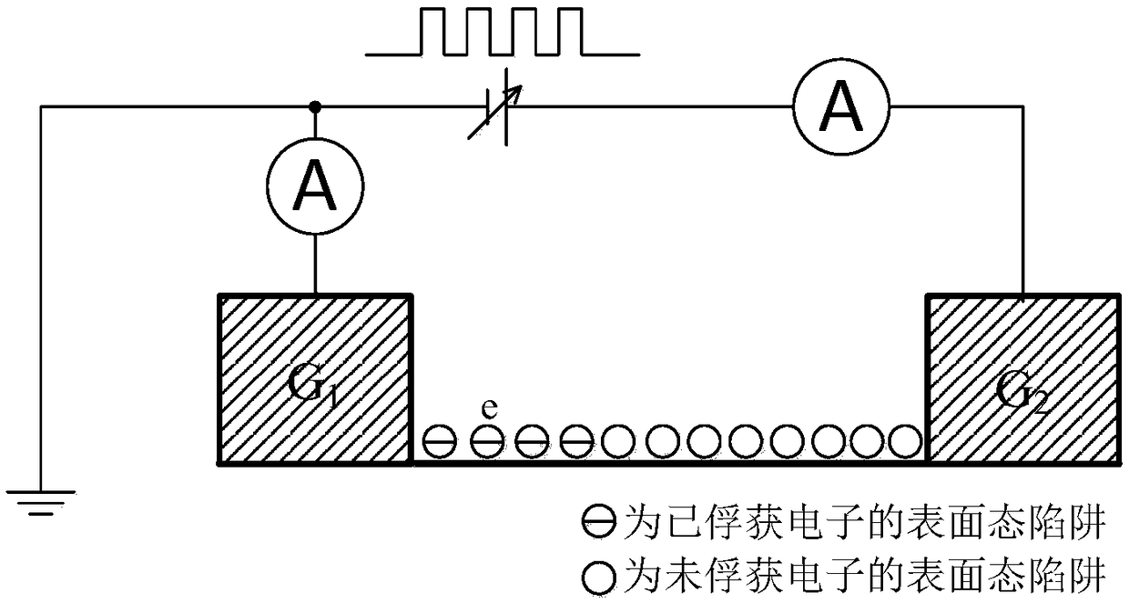
[0037] The devices under test involved in the present invention are three-terminal devices, including but not limited to HEMT devices, MOS devices and JBT devices. The three electrodes of the device under test are gate G, source S and drain D. Since the drain D is an ohmic contact electrode, when the device is working, electrons enter the channel region through the drain D, and then enter the gate G. In this process, electrons will be affected by the traps in the barrier region under the gate G; because the purpose of the present invention is to study the properties of the surface state traps of the device, if the device is directly tested, the traps in the barrier region under the gate G will be introduce...


PUM


Abstract

The present invention discloses a device surface state trap measurement method based on a frequency variable pulse technology. The objective of the invention is mainly to solve the problem that devicesurface state trap distribution cannot be measured in the prior art. The implementation scheme of the method comprises the following steps of: preparing two Schottky contact electrodes at a surface of semiconductor materials being the same as electrodes of tested devices, and completing preparation of a test pattern; applying pulse voltages with different frequencies to the test pattern, and measuring currents flowing through the two electrodes in the process of applying the voltages; and through calculation of a measurement result, obtaining the number of electrons trapped by the surface state traps of the test pattern, and taking an obtained test pattern result as distribution of surface state traps of the measurement device under different frequency voltages according to a feature thatthe test pattern and the tested device having the same surface state. The method provided by the invention is simple and high in test precision, can be used for technology optimization and reliability analysis of a heterojunction transistor.

Description

technical field [0001] The invention belongs to the technical field of microelectronic device testing, in particular to a method for measuring device surface state traps, which can be used for process optimization and reliability analysis of heterojunction transistors. Background technique [0002] From the first generation of semiconductor materials represented by silicon materials to the second generation of semiconductor materials represented by gallium arsenide materials, to the third generation of semiconductor materials represented by gallium nitride, many devices made of them The properties are closely related to the surface properties of semiconductors. [0003] Especially when the device is driven by high frequency and large signal, the output current swing decreases sharply, and the output power density decreases. This phenomenon is called the current collapse effect. As the most mature and convincing theory in the formation mechanism of the current collapse effec...

Claims


Application Information

Patent Timeline
Patent Type & Authority Patents(China)
IPC IPC(8): G01R31/26
CPCG01R31/2601G01R31/2648
Inventor 郑雪峰王士辉董帅帅吉鹏王颖哲杜鸣马晓华郝跃
Owner XIDIAN UNIV
Why Eureka
Try Eureka