Preparation method and structure of three-dimensional memory
A memory, three-dimensional technology, applied in the direction of electric solid devices, semiconductor devices, electrical components, etc., can solve the problems such as the increase of electrode resistance of the metal gate 17 and the thickness loss of the tungsten metal gate 17, and achieve the effect of increasing the thickness
- Summary
- Abstract
- Description
- Claims
- Application Information
AI Technical Summary
Problems solved by technology
Method used
Image

Examples
Embodiment 1
[0040] refer to Figure 10-14 As shown, Embodiment 1 of the present invention proposes a method for preparing a three-dimensional memory, which is characterized in that it includes the following steps:
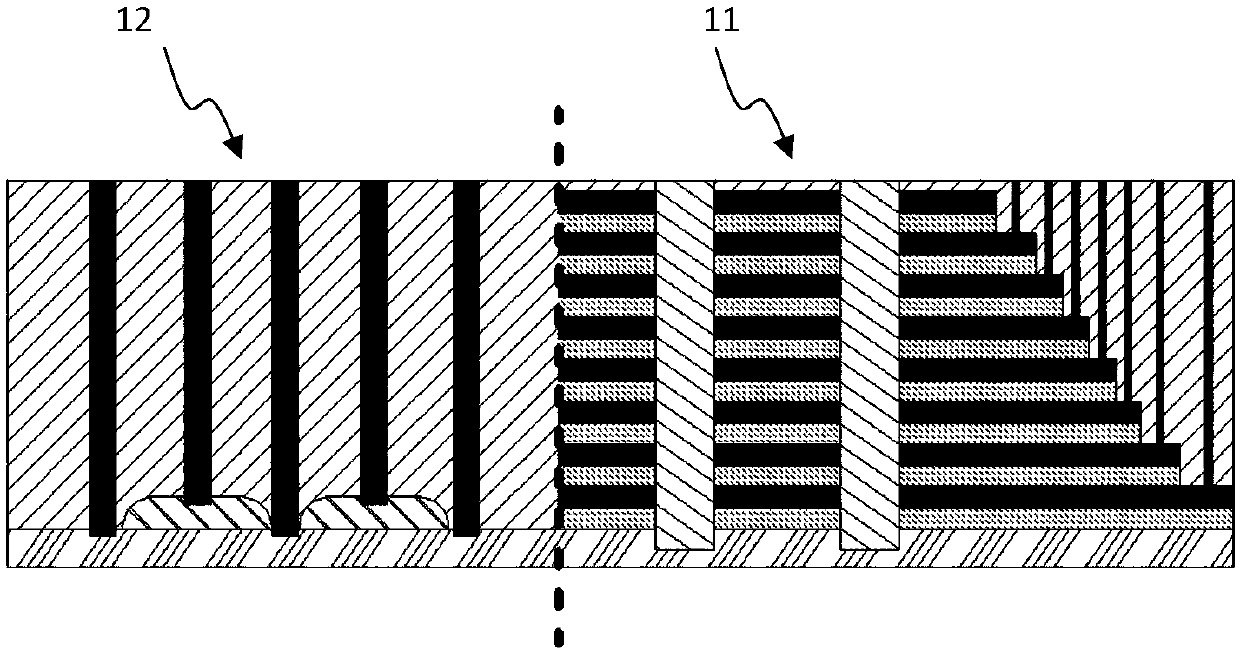
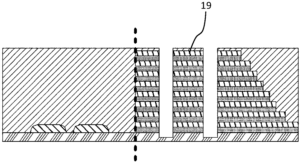
[0041] Such as Figure 10 As shown, a substrate 20 is provided, and an array storage area 21 and a peripheral circuit area 22 of a three-dimensional memory are formed on the substrate 20;
[0042] The display storage area 21 includes a multi-layer stack structure in which silicon oxide layers 23 and silicon nitride layers 24 are alternately formed on the substrate 20; the number of layers of the stack structure is greater than or equal to 48 layers, preferably 48 layers or 64 layers , 80 floors, 96 floors, 112 floors or 128 floors.
[0043] forming a storage core area 25 and a stepped area 26 with a multi-layer stack structure;
[0044] Such as Figure 10 As shown, a plurality of through holes 27 are formed in the storage core area 25;
[0045] Such as Figure 11 As shown,...
Embodiment 2
[0051] Embodiment 2 of the present invention proposes a method for preparing a three-dimensional memory, which is characterized in that it includes the following steps:
[0052] Such as Figure 10 As shown, a substrate 20 is provided, and an array storage area 21 and a peripheral circuit area 22 of a three-dimensional memory are formed on the substrate 20;
[0053] The display storage area 21 includes a multi-layer stack structure in which silicon oxide layers 23 and silicon nitride layers 24 are alternately formed on the substrate 20;
[0054] A multilayer stack structure is formed into a storage core region 25 and a step region 26; a step region 26 is formed on at least one side of the multilayer stack structure so that a part of the upper surface of each silicon nitride layer 24 is exposed to step area 26;
[0055] Such as Figure 10 As shown, an insulating layer 36 with a flat surface is formed on the substrate 20 to cover the peripheral circuit area 22 and the array st...
Embodiment 3
[0062] Embodiment 3 of the present invention proposes a method for manufacturing a three-dimensional memory. In this embodiment, parts different from the above embodiments will be described, and the same parts will not be repeated.
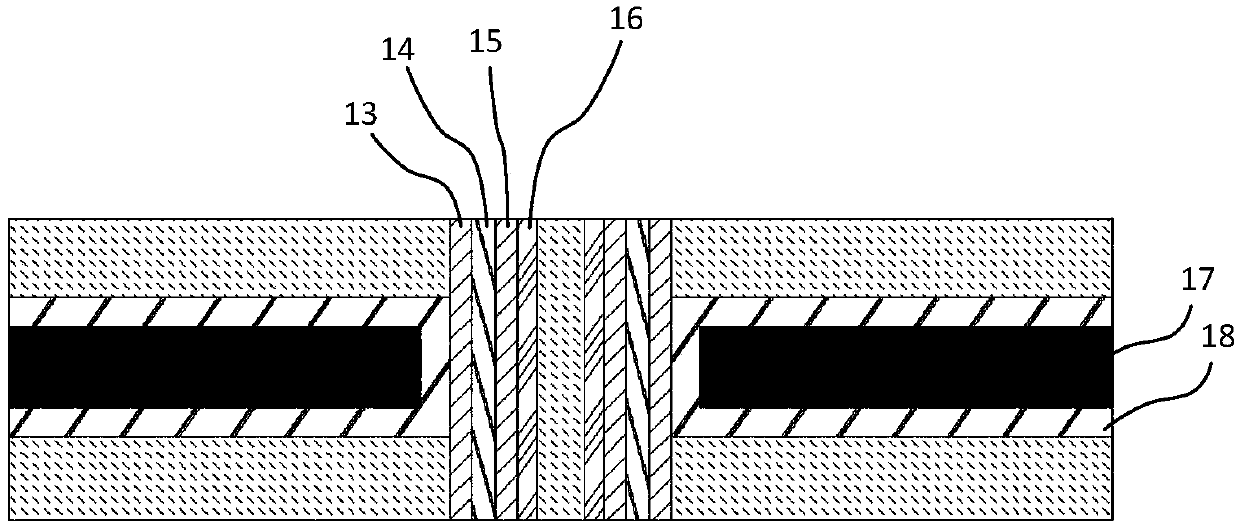
[0063] The forming of the contact hole 34 electrically connected to the peripheral circuit region 22 includes patterning the insulating layer 36 on the peripheral circuit region 22, etching and metal filling to form a contact hole 34 electrically connected to the peripheral circuit region 22. A plurality of first contact holes 34 .
[0064] The formation of the contact hole 35 electrically connected to the metal gate 33 includes patterning the insulating layer 26 on the array storage area 21, etching and filling with metal to form a contact hole 35 with each metal gate of the array storage area 21. A plurality of second contact holes 35 electrically connected to the gate 33 .
[0065] The metal material used for the metal filling is tungsten.
PUM
 Abstract
Description
Claims
Application Information
 - R&D
- Intellectual Property
- Life Sciences
- Materials
- Tech Scout
- Unparalleled Data Quality
- Higher Quality Content
- 60% Fewer Hallucinations
Browse by: Latest US Patents, China's latest patents, Technical Efficacy Thesaurus, Application Domain, Technology Topic, Popular Technical Reports.
© 2025 PatSnap. All rights reserved.Legal|Privacy policy|Modern Slavery Act Transparency Statement|Sitemap|About US| Contact US: help@patsnap.com