Semiconductor structure and formation method thereof

A semiconductor and isolation structure technology, which is applied in the field of semiconductor structure and its formation, can solve the problems of inconsistent fin width, easily affecting the performance of fin field effect transistors, inconsistent performance of fin field effect transistors, etc., and achieve the goal of suppressing the width of fins The effect of shrinking, reducing inconsistency, and improving consistency

Inactive Publication Date: 2018-02-23
SEMICON MFG INT (SHANGHAI) CORP +1
View PDF6 Cites 2 Cited by
  • Summary
  • Abstract
  • Description
  • Claims
  • Application Information

AI Technical Summary

Problems solved by technology

The width of the fin in the FinFET is very small, and a small change in the width of the fin will easily affect the performance of the FinFET
[0005] However, in the semiconductor structure formed in the prior art, the fin widths of different FinFETs are inconsistent, resulting in inconsistent performance of different FinFETs

Method used


Image

  • Semiconductor structure and formation method thereof
  • Semiconductor structure and formation method thereof
  • Semiconductor structure and formation method thereof

Examples


Embodiment Construction

[0033] There are many problems with the method of forming the semiconductor structure, including: inconsistent fin width and inconsistent transistor performance.

[0034] Combining with a method of forming a semiconductor structure, the reasons for the inconsistent width of the fins are analyzed:

[0035] Figure 1 to Figure 5 It is a structural schematic diagram of each step of a method for forming a semiconductor structure.

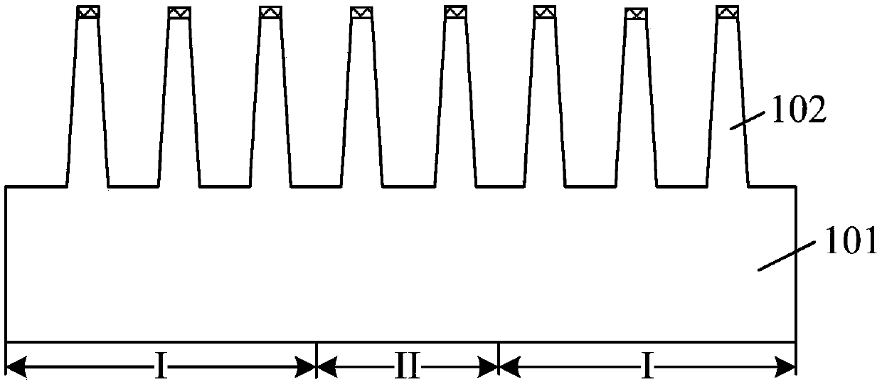
[0036] Please refer to figure 1 , providing a base, the base includes a substrate 101 and a fin 102 on the substrate 101 . The substrate includes: an isolation region II and device regions I located on both sides of the isolation region II.

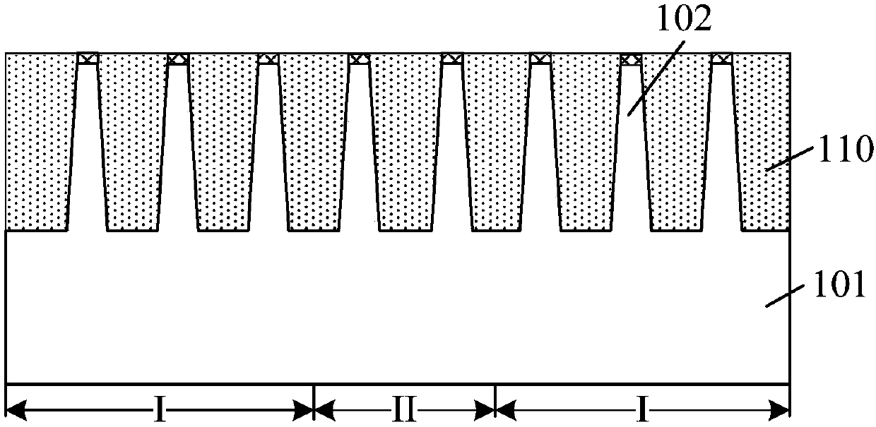
[0037] Please refer to figure 2 , forming an initial isolation structure 110 on the surface of the substrate 101 , and the initial isolation structure 110 covers the sidewall of the fin portion 102 .

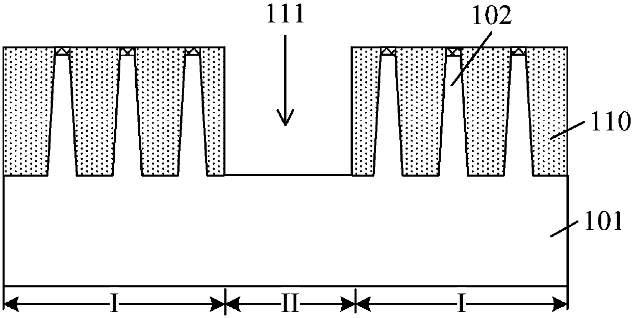
[0038] Please refer to image 3 , removing the fin portion 102 and the initial isolation structure 110 on t...


PUM


Abstract

The invention provides a semiconductor structure and a formation method thereof. The formation method comprises the following steps: providing a substrate, wherein the substrate comprises device areasand an isolation area, the device area substrate having fin portions and an initial isolation structure, the initial isolation structure covering side walls of the fin portions, the side walls, adjacent to the isolation area, of the initial isolation structure and the isolation area substrate forming an isolation groove; carrying out ion implantation on the side walls of the isolation groove to inject doping ions, and forming a barrier layer on the surfaces of the side walls of the isolation groove; after ion implantation, forming an isolation layer filling the isolation groove; and after forming the isolation layer, etching the initial isolation structure to expose the top portions and partial side wall surfaces of the fin portions and forming an isolation structure. The formation methodcan reduce the problem of inconsistency of fin portion width, and thus the performance of the semiconductor structure is improved.

Description

technical field [0001] The invention relates to the technical field of semiconductor manufacturing, in particular to a semiconductor structure and a forming method thereof. Background technique [0002] With the rapid development of semiconductor manufacturing technology, semiconductor devices are developing towards higher component density and higher integration. Transistors are currently being widely used as the most basic semiconductor devices. As the component density and integration of semiconductor devices increase, the size of transistors is also getting smaller. [0003] A Fin Field Effect Transistor (FinFET) has intersecting fins like fish fins, which can improve the integration of semiconductor devices. Moreover, the gate structure of the fin field effect transistor can control the channel of the transistor from both sides of the fin, thereby increasing the control of the carriers in the channel of the transistor, which is beneficial to reducing the leakage curre...

Claims


Application Information

Patent Timeline
Patent Type & Authority Applications(China)
IPC IPC(8): H01L21/336H01L29/78
CPCH01L29/66H01L29/785
Inventor 周飞
Owner SEMICON MFG INT (SHANGHAI) CORP
Why Eureka
Try Eureka