
Flexible LED manufacture process and flexible LED structure

A light-emitting diode, flexible technology, applied in the direction of electrical components, circuits, semiconductor devices, etc., can solve the problems of not being able to respond to the display surface, unable to achieve flexible effects, uneven playing surface, etc.

Pending Publication Date: 2018-03-02
GUANGZHOU HKUST FOK YING TUNG RES INST
View PDF17 Cites 6 Cited by
  • Summary
  • Abstract
  • Description
  • Claims
  • Application Information

AI Technical Summary

Problems solved by technology

However, no matter how it improves its heat dissipation efficiency or finds the most suitable bonding force between metals, the light-emitting diodes produced by the above-mentioned method cannot achieve the effect of being flexible when they are displayed; that is, , the structure produced by this method, because the overall structure presents a rigid structure, cannot cope with the uneven playing surface of the display surface; that is to say, the above structure can only be placed on a flat playing surface

Method used


Image

  • Flexible LED manufacture process and flexible LED structure
  • Flexible LED manufacture process and flexible LED structure
  • Flexible LED manufacture process and flexible LED structure

Examples


Embodiment Construction

[0054] The technical solutions in the embodiments of the invention will be clearly and completely described below in conjunction with the accompanying drawings in the embodiments of the invention. Obviously, the described embodiments are only some, not all, embodiments of the invention. Based on the embodiments of the present invention, all other embodiments obtained by persons of ordinary skill in the art without making creative efforts fall within the protection scope of the present invention.

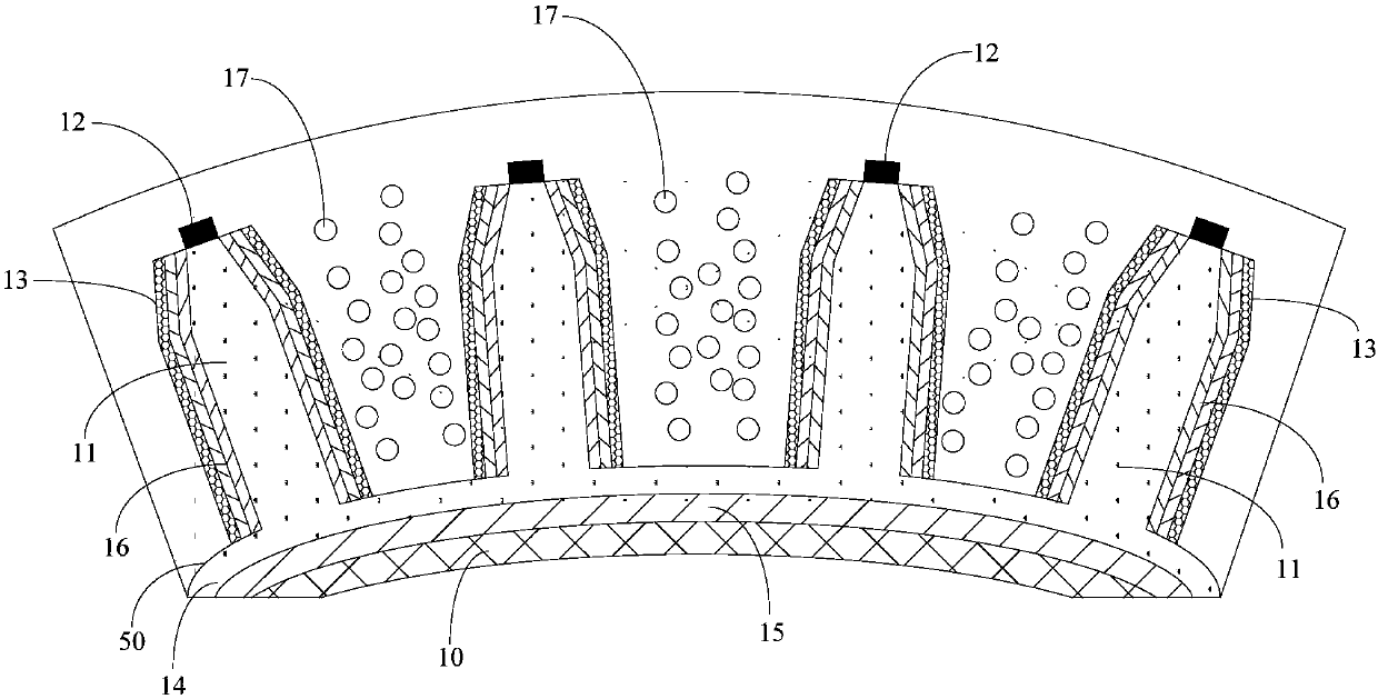
[0055] see figure 1 A flexible light emitting diode structure provided in an embodiment of the present invention mainly includes a flexible substrate 10, a gallium nitride nanocolumn 11 disposed on the flexible substrate 10, a gallium nitride nanocolumn 11 disposed on the flexible substrate 10 The current blocking layer 12 on the free end of the gallium nitride nanorod 11 and the transparent conductive layer 13 disposed on the column body of the gallium nitride nanorod 11 . Among th...


PUM

PropertyMeasurementUnit
dielectric lossaaaaaaaaaa

Abstract

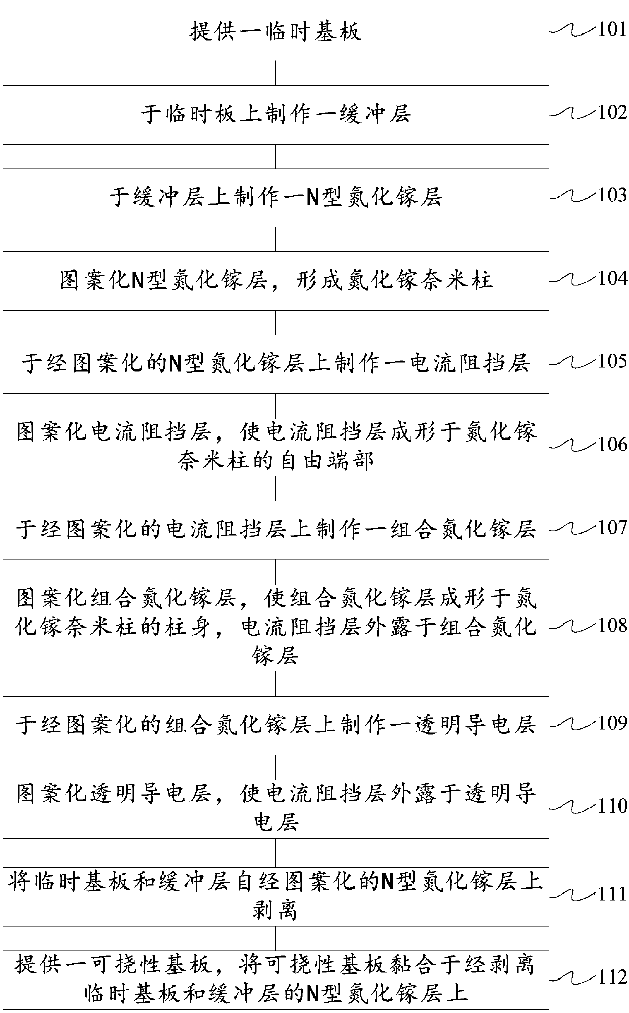
The invention discloses a flexible LED manufacture process and a flexible LED structure. The flexible LED manufacture process comprises steps of forming a buffer layer on a temporary substrate, forming an N-type GaN layer on the buffer layer, patterning the N-type GaN layer, forming a GaN nano column, forming a silicon nitride layer on the patterned GaN layer, forming a current barrier layer on the silicon nitride layer, forming an insulating layer on the patterned current barrier layer, exposing the current barrier layer and the patterned GaN layer to the insulating layer, form a GaN layer, forming an indium tin conductive layer on the patterned GaN layer and the insulating layer, separating the temporary substrate and the buffer layer from the aforementioned mixed structure, fully mixingorganic silicon and the quantum dots to fill a mixed structure separated from the temporary substrate and the buffer layer, and bonding soft polyimide to the mixed structure separated from the temporary substrate and the buffer layer.

Description

technical field [0001] The invention relates to the technical field of semiconductors, in particular to a flexible light-emitting diode manufacturing process and its structure. Background technique [0002] Gallium Nitride (GaN) is a semiconductor material with a wide bandgap (3.4 electron volts). Many new optoelectronic applications can be developed by utilizing the unique properties of GaN semiconductor materials to excite blue light. At present, GaN optoelectronic devices and electronic devices have good development prospects in the application fields of optical storage, laser printing, high-brightness LEDs and wireless base stations. [0003] Due to the nature of the GaN material itself, such as: high melting temperature and high saturation vapor pressure of nitrogen during preparation, it is difficult to obtain a good-quality GaN single crystal substrate, so that homogeneous large-area GaN single crystal Crystal is difficult. In GaN epitaxial process, sapphire (Al 2...

Claims


Application Information

Patent Timeline
Patent Type & Authority Applications(China)
IPC IPC(8): H01L33/32H01L33/44H01L33/20H01L33/00
CPCH01L33/0075H01L33/20H01L33/32H01L33/44
Inventor 佘庆威郭浩中黄陈嵩文朱国雄林志豪
Owner GUANGZHOU HKUST FOK YING TUNG RES INST
Learn More