Removal method for protection layer on surface of device
What is AI technical title?
AI technical title is built by Patsnap AI team. It summarizes the technical point description of the patent document.
A device surface and protective layer technology, applied in semiconductor/solid-state device manufacturing, electrical components, circuits, etc., can solve problems such as incomplete removal of protective layer, damage to the metal layer of the device, etc.
Active Publication Date: 2018-03-06
SEMICON MFG INT (SHANGHAI) CORP +1
View PDF4 Cites 0 Cited by
Summary
Abstract
Description
Claims
Application Information
AI Technical Summary
This helps you quickly interpret patents by identifying the three key elements:
Problems solved by technology
Method used
Benefits of technology
Problems solved by technology
[0005] The technical problem to be solved by the present invention is to provide a method for removing the protective layer on the surface of the device to solve the problems in the prior art that the removal of the protective layer on the surface of the device is incomplete and the metal layer on the surface of the device is damaged
Method used
Image
Click on the blue label to locate the original text in one second.
Reading with bidirectional positioning of images and text.
Examples
Embodiment 1
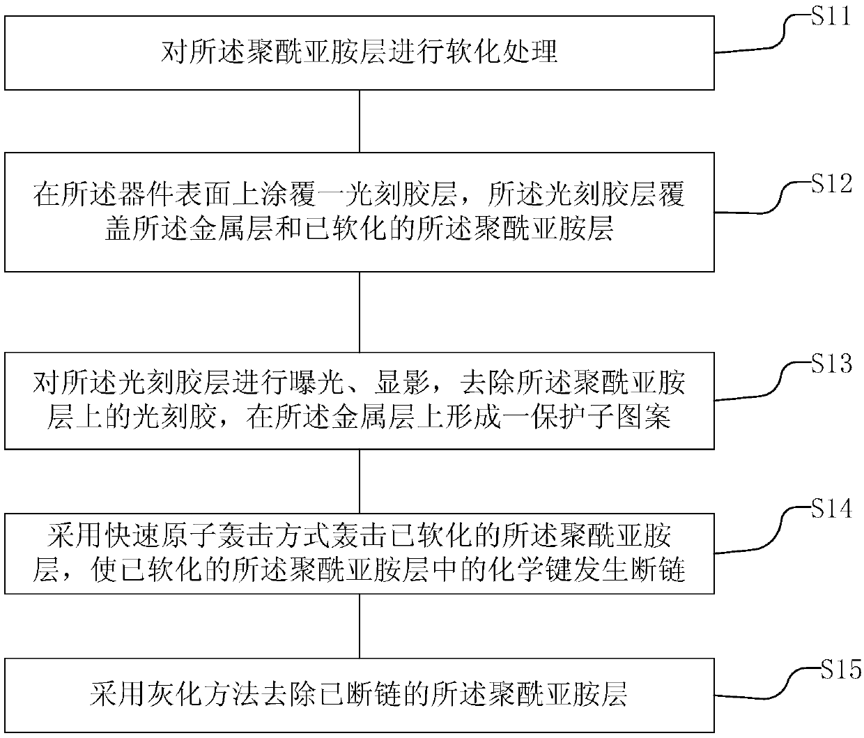
[0044] see figure 2 , which shows a specific flow chart of the removal method of the polyimide layer described in Embodiment 1 of the present invention, the removal method includes:
[0046] Step S12, coating a photoresist layer on the surface of the device, the photoresist layer covering the metal layer and the softened polyimide layer;
[0047] Step S13, exposing and developing the photoresist layer, removing the photoresist on the polyimide layer, and forming a protective sub-pattern on the metal layer;
[0048]Step S14, using fast atom bombardment to bombard the softened polyimide layer, so that the chemical bonds in the softened polyimide layer are broken;
[0049] Step S15 , removing the broken polyimide layer by ashing method.
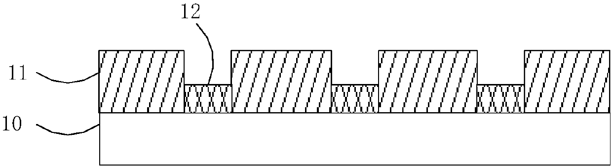
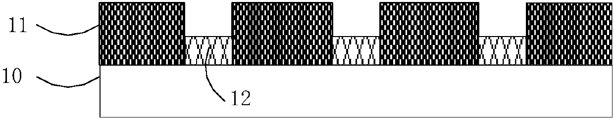
[0050] Next, in order to describe the removal method described in this embodiment more clearly, please refer to Figure 3-Figure 7 , which shows a schematic structural diagram corresponding ...
Embodiment 2
[0062] see Figure 8 , which shows a specific flow chart of the removal method of the polyimide layer described in Embodiment 2 of the present invention, the removal method comprising:
[0063] Step S21, coating a photoresist layer on the surface of the device, the photoresist layer covering the metal layer and the polyimide layer;
[0064] Step S22, exposing and developing the photoresist layer, removing the photoresist on the polyimide layer, and forming a protective sub-pattern on the metal layer;
[0065] Step S23, softening the polyimide layer;
[0066] Step S24, using fast atom bombardment to bombard the softened polyimide layer, so that the chemical bonds in the softened polyimide layer are broken;
[0067] Step S25 , using an ashing method to remove the broken polyimide layer.
[0068] see Figure 9 to Figure 11 , the reference numerals denote the same Figure 3-Figure 7 The same expression and the same structure in the removal method of the first embodiment, the ...
PUM
Abstract
The invention discloses a removal method for a protection layer on a surface of a device. The removal method comprises the steps of softening the protection layer; bombarding the softened protection layer by employing a rapid atomic bombardment mode so that a chemical bond in the softened protection layer is broken; and removing the broken protection layer by an ashing method. By softening the protection layer, the hardness of the cured protection layer is reduced; with the adoption of the rapid atomic bombardment mode, the chemical bond of a protection layer material is broken, more broken chemical bonds are formed, so that the property of the protection layer is changed, and the subsequent ashing process is facilitated; and finally, the broken protection layer material can be easily removed by an ashing mode. With the adoption of the removal method provided by the invention, the protection layer can be completely removed, and the subsequent rework process and the electric property ofan electrical appliance cannot be affected.
Description
technical field [0001] The invention relates to the field of integrated circuit manufacturing, in particular to a method for removing a protective layer on a device surface. Background technique [0002] In the semiconductor process, polyimide (Polyimide, PI) is more and more widely used, such as metal-insulator-metal (Metal Insulator Metal, MIM) capacitor production, photoresist materials, and protective layers. Polyimide (Polyimide, PI) is an organic polymer material, which has the characteristics of high temperature resistance, radiation resistance, good insulation performance, corrosion resistance, and stable chemical properties. The amine resin is used as a protective layer to isolate the device from external water vapor and dust and other pollutants, thereby ensuring the insulation and other characteristics of the device. [0003] Then, due to the increasingly high requirements for polyimide, it often occurs in the actual process that the polyimide layer needs to be r...
Claims
Application Information
Patent Timeline
Application Date:The date an application was filed.
Publication Date:The date a patent or application was officially published.
First Publication Date:The earliest publication date of a patent with the same application number.
Issue Date:Publication date of the patent grant document.
PCT Entry Date:The Entry date of PCT National Phase.
Estimated Expiry Date:The statutory expiry date of a patent right according to the Patent Law, and it is the longest term of protection that the patent right can achieve without the termination of the patent right due to other reasons(Term extension factor has been taken into account ).
Invalid Date:Actual expiry date is based on effective date or publication date of legal transaction data of invalid patent.

