Preparation method of gallium nitride epitaxial structure based on molybdenum disulfide-graphene composite buffer layer

A technology of graphene composite and molybdenum disulfide, which is applied in the field of optoelectronics, can solve problems such as the difficulty in effectively alleviating the lattice mismatch of the substrate, the inability to grow the aluminum nitride layer, and the poor quality of nitride materials, and achieve good and high-precision thin films Growth quality, good thickness controllability, stress reduction effect

Active Publication Date: 2018-03-06
INST OF ELECTRONICS ENG CHINA ACAD OF ENG PHYSICS
View PDF6 Cites 2 Cited by
  • Summary
  • Abstract
  • Description
  • Claims
  • Application Information

AI Technical Summary

Problems solved by technology

[0006] However, the shortcomings of this method are: magnetron sputtering aluminum nitride, the sputtering speed is fast, but the quality of the film is poor, there are many impurities, and further heat treatment is required after the sputtering growth film is formed, so this method cannot grow better aluminum nitride layers, resulting in poor quality nitride materials obtained
However, the thickness of graphene is very thin, and it is difficult to effectively alleviate the lattice mismatch between the substrate and GaN.

Method used


Image

  • Preparation method of gallium nitride epitaxial structure based on molybdenum disulfide-graphene composite buffer layer
  • Preparation method of gallium nitride epitaxial structure based on molybdenum disulfide-graphene composite buffer layer
  • Preparation method of gallium nitride epitaxial structure based on molybdenum disulfide-graphene composite buffer layer

Examples


Embodiment 1

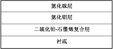
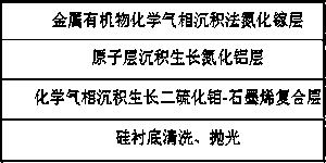
[0037] A method for preparing a gallium nitride epitaxial structure based on a molybdenum disulfide-graphene composite buffer layer, comprising the following method steps:

[0038] A, cleaning the silicon substrate;

[0039] B, growing a molybdenum disulfide-graphene composite layer on a silicon substrate;

[0040] C, utilize atomic layer deposition to grow a layer of aluminum nitride layer on the molybdenum disulfide-graphene composite layer;

[0041] D. A gallium nitride layer is grown on the aluminum nitride layer by metal-organic chemical vapor deposition.

Embodiment 2

[0043] A method for preparing a gallium nitride epitaxial structure based on a molybdenum disulfide-graphene composite buffer layer, comprising the following method steps:

[0044] A, cleaning the silicon substrate;

[0045] B, growing a molybdenum disulfide-graphene composite layer on a silicon substrate;

[0046] C, utilize atomic layer deposition to grow a layer of aluminum nitride layer on the molybdenum disulfide-graphene composite layer;

[0047] D. A gallium nitride layer is grown on the aluminum nitride layer by metal-organic chemical vapor deposition.

[0048] In step A, specifically:

[0049] The silicon substrate was washed three times successively with ethanol and deionized water, washed with dilute hydrofluoric acid for 5 minutes, rinsed with deionized water, and dried with nitrogen gas to obtain a silicon substrate.

Embodiment 3

[0051] A method for preparing a gallium nitride epitaxial structure based on a molybdenum disulfide-graphene composite buffer layer, comprising the following method steps:

[0052] A, cleaning the silicon substrate;

[0053] B, growing a molybdenum disulfide-graphene composite layer on a silicon substrate;

[0054] C, utilize atomic layer deposition to grow a layer of aluminum nitride layer on the molybdenum disulfide-graphene composite layer;

[0055] D. A gallium nitride layer is grown on the aluminum nitride layer by metal-organic chemical vapor deposition.

[0056] In step A, specifically:

[0057] The silicon substrate was washed three times successively with ethanol and deionized water, washed with dilute hydrofluoric acid for 10 minutes, rinsed with deionized water, and dried with nitrogen gas to obtain a silicon substrate.


PUM

PropertyMeasurementUnit
thicknessaaaaaaaaaa
thicknessaaaaaaaaaa
thicknessaaaaaaaaaa

Abstract

The invention relates to a preparation method of a gallium nitride epitaxial structure based on a molybdenum disulfide-graphene composite buffer layer, and belongs to the technical field of photoelectronics. The preparation method comprises the steps of performing cleaning on a silicon substrate; enabling a molybdenum disulfide-graphene composite layer to be grown on the silicon substrate; enabling an aluminum nitride layer to be grown on the molybdenum disulfide-graphene composite layer by adopting an atomic layer deposition method; and enabling a gallium nitride layer to be grown on the aluminum nitride layer by adopting a metal organic chemical vapor deposition method, and the like. By adopting the molybdenum disulfide-graphene composite layer as the buffer layer between the silicon substrate and the GaN epitaxial layer, the problems of defect malposition, cracks and the like caused by high lattice mismatch and thermal mismatch between the substrate and the epitaxial layer can be solved, the stress between the substrate and the epitaxial material can be lowered effectively, and the GaN epitaxial layer quality is improved.

Description

technical field [0001] The invention relates to a preparation method of a gallium nitride epitaxial structure, more specifically, the invention relates to a preparation method of a gallium nitride epitaxial structure based on a molybdenum disulfide-graphene composite buffer layer, belonging to the field of optoelectronic technology. Background technique [0002] GaN material has received more and more attention as a new type of semiconductor material. As a representative material of the third-generation semiconductor, gallium nitride has excellent electrical and optical properties. It has the advantages of wide bandgap, direct bandgap, high temperature and high pressure resistance, and high electron mobility. It is used in the fields of electronic devices and optoelectronic devices. It has a wide range of applications, so the preparation of high-quality gallium nitride is the key to the preparation of the above devices. [0003] Graphene is a new two-dimensional nanomateria...

Claims


Application Information

Patent Timeline
Patent Type & Authority Applications(China)
IPC IPC(8): H01L21/02
CPCH01L21/02052H01L21/02381H01L21/02444H01L21/02458H01L21/02485H01L21/02502H01L21/0254H01L21/0262
Inventor 王文杰李沫李俊泽张建杨浩军谢武泽邓泽佳代刚张健
Owner INST OF ELECTRONICS ENG CHINA ACAD OF ENG PHYSICS
Why Eureka
Try Eureka