

LED epitaxial structure and preparation method thereof
A technology of epitaxial structure and nucleation structure, applied in semiconductor devices, electrical components, circuits, etc., can solve problems such as poor light extraction efficiency, uneven coarsening yield, and low refractive index
- Summary
- Abstract
- Description
- Claims
- Application Information
AI Technical Summary
Problems solved by technology
Method used
Image

Examples
Embodiment 1
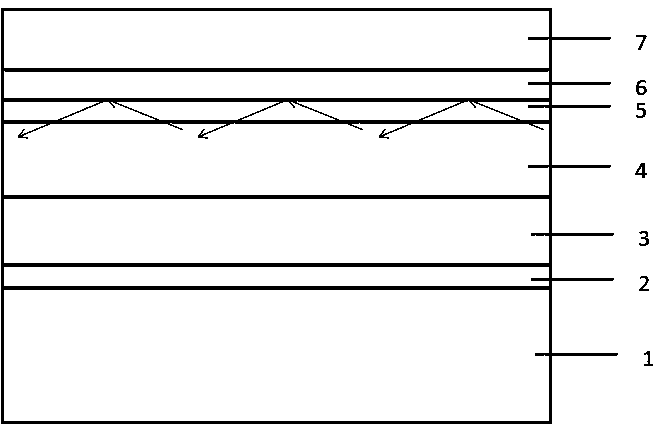
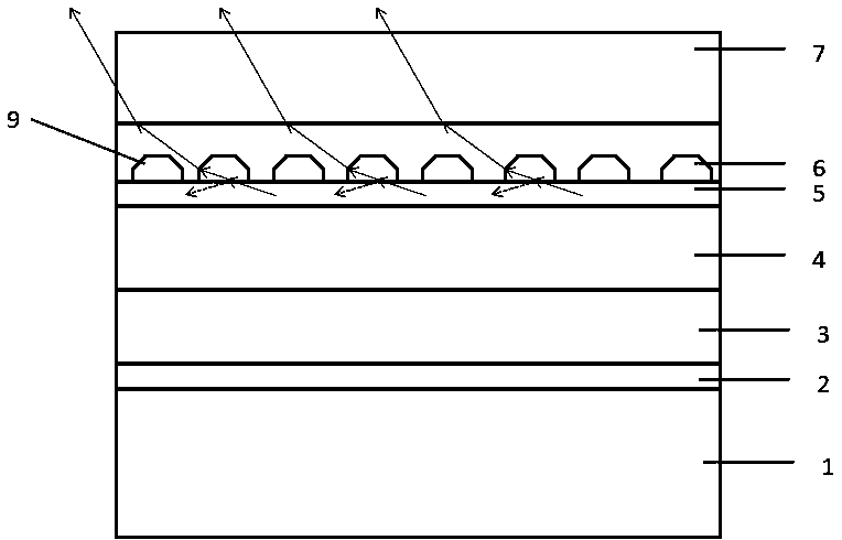
[0038] This implementation provides a kind of LED epitaxial structure, refer to the attached figure 2 The epitaxial structure includes a substrate 1, a buffer layer 2, a first semiconductor layer 3, a multi-quantum well light-emitting layer 4, a final barrier layer 5, and a plurality of discontinuously arranged island structures 9 located on the substrate 1 in sequence. , the electron blocking layer 6 and the second semiconductor layer 7 .
[0039] The discontinuously arranged island-like structures 9 are 3D island-like structures 9 whose shape is conical or truncated conical or yurt or polygonal prism or a combination of any two, three or four of the aforementioned shapes. In this embodiment, as attached figure 2 As shown, the shape of the island structures 9 is a combination of polygonal columns and polygonal pyramids, and the distance between the bottom of adjacent island structures 9 is greater than the distance between the tops, so that the light entering the island st...
Embodiment 2
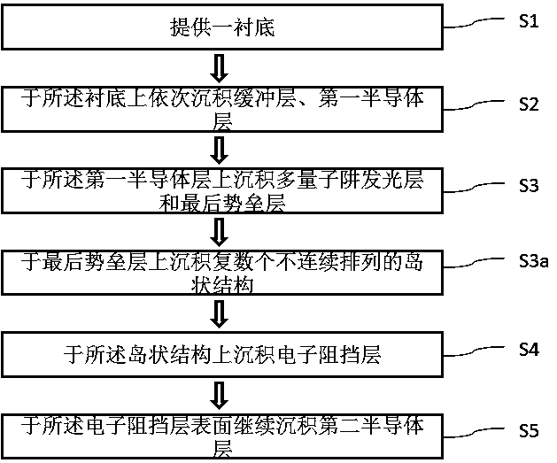
[0044] The embodiment of the present invention proposes a method for preparing an LED epitaxial structure, which is suitable for manufacturing the LED epitaxial structure provided in Example 1. Please refer to the attached image 3 , the preparation method comprises:
[0045] Step 1, first provide a substrate 1, the substrate 1 is a patterned substrate 1, specifically a sapphire patterned substrate 1;
[0046] Step 2, sequentially depositing a buffer layer 2 and a first semiconductor layer 3 on the substrate 1;
[0047] The buffer layer 2 is a GaN buffer layer 2 or an AlN buffer layer 2 or an AlGaN buffer layer 2, and the first semiconductor layer 3 is an N-type layer, which is mainly used to provide electrons.
[0048] Step 3, depositing a multi-quantum well light-emitting layer 4 and a final barrier layer 5 on the first semiconductor layer 3;
[0049] The multi-quantum well light-emitting layer 4 is a superlattice structure in which GaN quantum barrier layers and InGaN quant...
Embodiment 3
[0058] See attached Figure 4 The difference between the LED epitaxial structure provided in this embodiment and the LED epitaxial structure provided in the embodiment is that there are a plurality of nucleation structures serving as the core of the island structure 9 between the barrier layer 5 and the island structure 9 8. The nucleation structure 8 serves as the nucleation center of the island structure 9 , and its size is smaller than that of the island structure 9 .
[0059] Specifically, the LED epitaxial structure provided in this embodiment includes: a substrate 1, a buffer layer 2 located on the substrate 1, a first semiconductor layer 3, a multi-quantum well light-emitting layer 4, a final barrier layer 5, and a nucleation structure 8. Island structure 9 , electron blocking layer 6 and second semiconductor layer 7 .
[0060] Wherein, the material of the nucleation structure 8 is a magnesium nitride compound, the refractive index of the island structure 9 is greater ...
PUM
 Abstract
Description
Claims
Application Information