Bracket-shaped grid-control source drain resistive two-way switch transistor and manufacturing method thereof

A bidirectional switch and transistor technology, applied in the manufacture of semiconductor/solid-state devices, semiconductor devices, electrical components, etc., can solve the loss of control of the gate, the decline of the switching performance of the device, and the reduction of the gate electrode's ability to control the drain and source regions, etc. question

Active Publication Date: 2018-03-09
深圳市麦思浦半导体有限公司
View PDF5 Cites 0 Cited by
  • Summary
  • Abstract
  • Description
  • Claims
  • Application Information

AI Technical Summary

Problems solved by technology

However, in order to realize the switching characteristics of the gate electrode of the usual Schottky barrier field effect transistor (the gate electrode is forward-conducting and reverse-blocking or reverse-conducting and forward-blocking), it is necessary to perform a specific conductivity type on the source or drain region of the device. impurity doping, which makes it difficult to achieve a good Schottky contact between the source electrode and the source region, between the drain electrode and the drain region, and the doping of the source region and the drain region makes the gate electrode to the drain The control ability of the r

Method used


Image

  • Bracket-shaped grid-control source drain resistive two-way switch transistor and manufacturing method thereof
  • Bracket-shaped grid-control source drain resistive two-way switch transistor and manufacturing method thereof
  • Bracket-shaped grid-control source drain resistive two-way switch transistor and manufacturing method thereof

Examples


Embodiment Construction

[0058] Below in conjunction with accompanying drawing, the present invention will be further described:

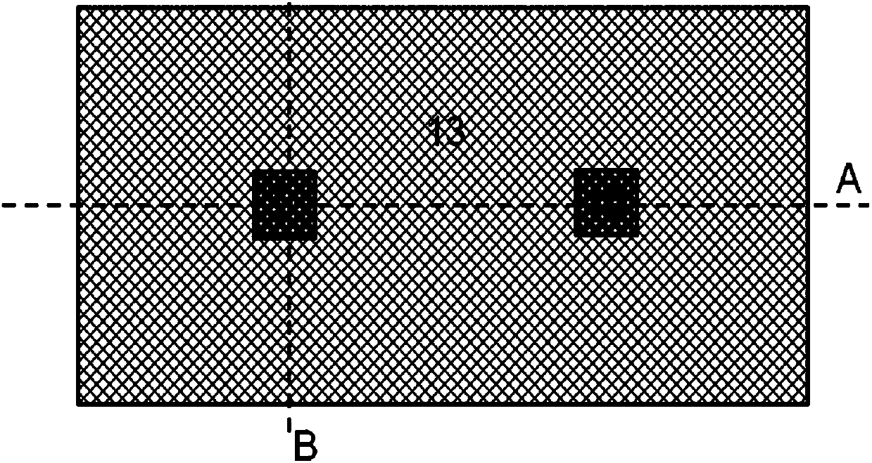
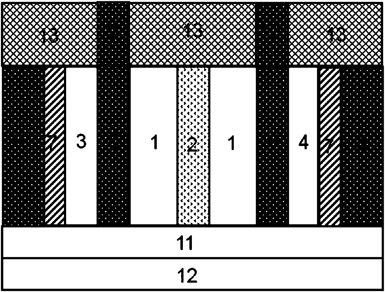
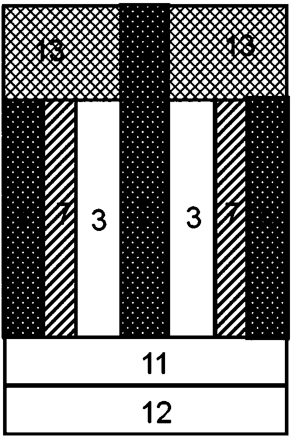
[0059] Such as figure 1 , figure 2 with image 3 As shown, a bracket-shaped gate-controlled source-drain resistance variable bidirectional switch transistor includes a silicon substrate 12 of an SOI wafer, and the top of the silicon substrate 12 of the SOI wafer is a substrate insulating layer 11 of the SOI wafer; Above the round substrate insulating layer 11 is a single crystal silicon film 1, heavily doped region 2, source-drain interchangeable intrinsic region a 3, source-drain interchangeable intrinsic region b 4, metal source-drain interchangeable Region a5, metal source-drain interchangeable region b6, gate electrode insulating layer 7, bracket gate electrode 8 and partial regions of insulating dielectric barrier layer 13;

[0060] Among them, the heavily doped region 2 is located in the middle part of the single crystal silicon film 1, and the metal source-drain...


PUM


Abstract

The invention relates to a bracket-shaped grid-control source drain resistive two-way switch transistor and a manufacturing method thereof. According to the bracket-shaped grid-control source drain resistive two-way switch transistor, a device is structurally characterized by comprising bracket grids symmetrical left and right and has strong grid control capability and can control a metal source and drain interchangeable area as a source area or a drain area by adjusting a source and drain interchangeable electrode voltage to change the tunneling current direction. The bracket-shaped grid-control source drain resistive two-way switch transistor has the advantages of being low in static power and reverse leakage current, high in grid control capacity, low in subthreshold value swing and capable of achieving the two-way switching function. Compared with an ordinary MOSFETs type device, the tunneling effect is used for achieving a more excellent switching characteristic. Compared with anordinary tunneling field effect transistor, the bracket-shaped grid-control source drain resistive two-way switch transistor has the interchangeable source and drain two-way symmetrical switching characteristic with which the ordinary tunneling field effect transistor lacks, and therefore the bracket-shaped grid-control source drain resistive two-way switch transistor is suitable for application and popularization.

Description

technical field [0001] The invention relates to the field of ultra-large-scale integrated circuit manufacturing, in particular to a bracket-shaped gate-controlled source-drain resistance variable bidirectional switch transistor with low leakage current suitable for low-power integrated circuit manufacturing and a manufacturing method thereof. Background technique [0002] According to the requirements of Moore's law, MOSFETs, the basic unit of integrated circuits, must become smaller and smaller in size. The resulting problem is not only the increase in the difficulty of the manufacturing process, but also the adverse effects of the device itself caused by the smaller size. highlight. Due to the limitation of the physical mechanism of current generation of MOSFETs used in integrated circuit design, the subthreshold swing cannot be lower than 60mV / dec. [0003] When ordinary tunneling field effect transistors are used as switching devices, the tunneling mechanism of carriers...

Claims


Application Information

Patent Timeline
IPC IPC(8): H01L29/78H01L21/336
CPCH01L29/66477H01L29/7839
Inventor 刘溪夏正亮靳晓诗
Owner 深圳市麦思浦半导体有限公司
Why Eureka
Try Eureka