Flash memory
A flash memory, memory cluster technology, used in static memory, read-only memory, memory systems, etc., to solve problems such as threshold voltage changes and data no longer being read correctly
- Summary
- Abstract
- Description
- Claims
- Application Information
AI Technical Summary
Problems solved by technology
Method used
Image

Examples
Embodiment 1
[0048]
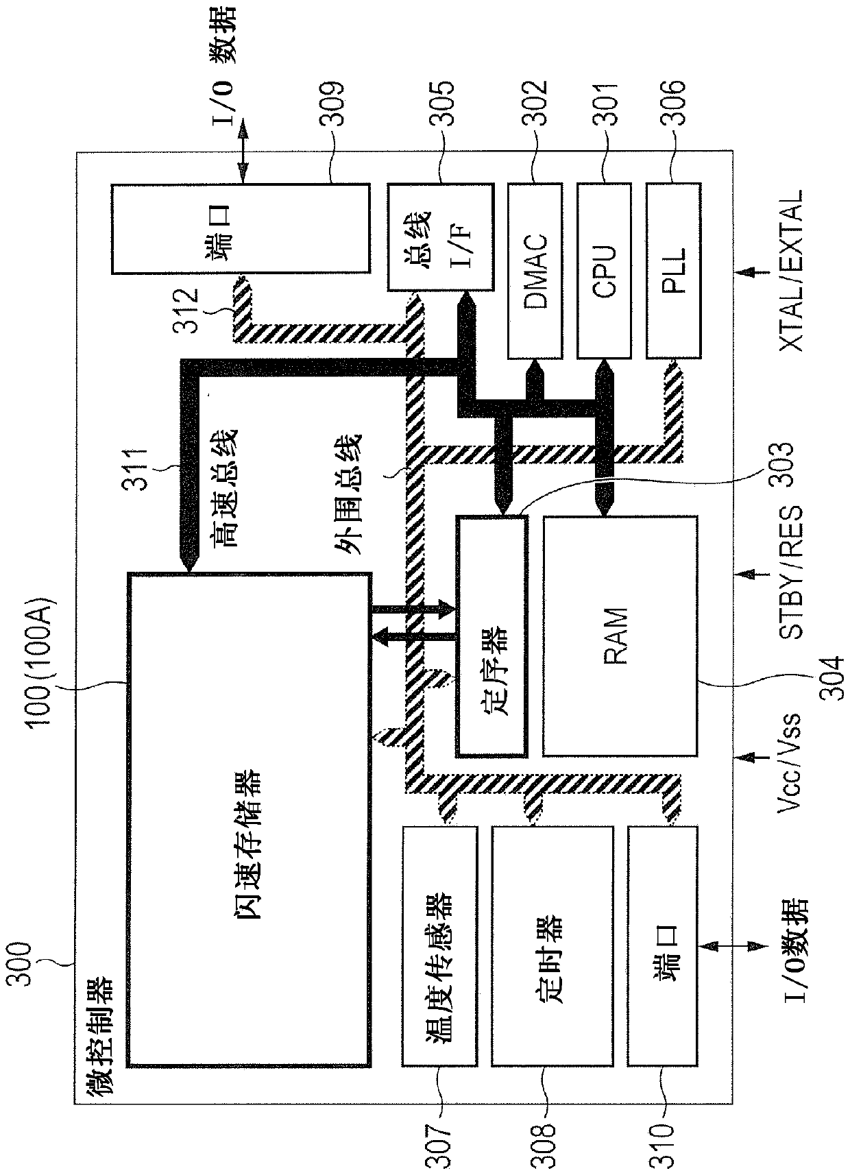
[0049] figure 1 is a block diagram showing an example of the structure of a flash memory-mounted microcontroller according to Embodiment 1 of the present invention. Such as figure 1 As shown, the microcontroller 300 includes a flash memory 100, a CPU (Central Processing Unit) 301, a DMAC (Direct Memory Access Controller) 302, a sequencer 303, a RAM (Random Access Memory) 304, a bus interface (bus I / F) 305 , PLL (Phase Locked Loop) 306 , temperature sensor 307 , timer 308 , ports 309 and 310 , high-speed bus 311 and peripheral bus 312 .
[0050] The flash memory 100 , CPU 301 , DMAC 302 , sequencer 303 , RAM 304 , and bus interface 305 are coupled to each other via a high-speed bus 311 , and data input / output among these units is performed via the high-speed bus 311 . With the high-speed bus 311 , data input / output is performed at a higher speed than the peripheral bus 312 .
[0051] Flash memory 100 , bus interface 305 , PLL 306 , temperature sensor 307 , timer 308...
Embodiment 2
[0165] Next, Example 2 of the present invention will be described. The present embodiment explains the processing related to the refresh operation in which data 0 margin reading is performed in addition to data 1 margin reading. Hereinafter, descriptions of contents overlapping with the above-described Embodiment 1 are omitted in principle.
[0166] Figure 15 is a flowchart showing a flash memory refresh method according to Embodiment 2 of the present invention. In this example, if Figure 15 As shown, the refresh operation of the flash memory is performed through steps S1001 to S1052 and steps S2060 to S2080.
[0167] In step S1030, when the controller 120 determines that the data read in the first reading step S1010 is the same as the data read in the second reading step S1020 (Yes), step S2060 is performed.
[0168] Step S2060 is a third reading step in which the controller 120 executes data 0 margin reading. Specifically, the sense amplifier SA performs data 0 margin...
Embodiment 3
[0180] Next, Example 3 of the present invention will be described. This embodiment illustrates a flash memory of a complementary system in which data is stored in a pair of memory cells. Hereinafter, descriptions of contents overlapping with the above-described Embodiment 1 and Embodiment 2 are omitted in principle.
[0181]
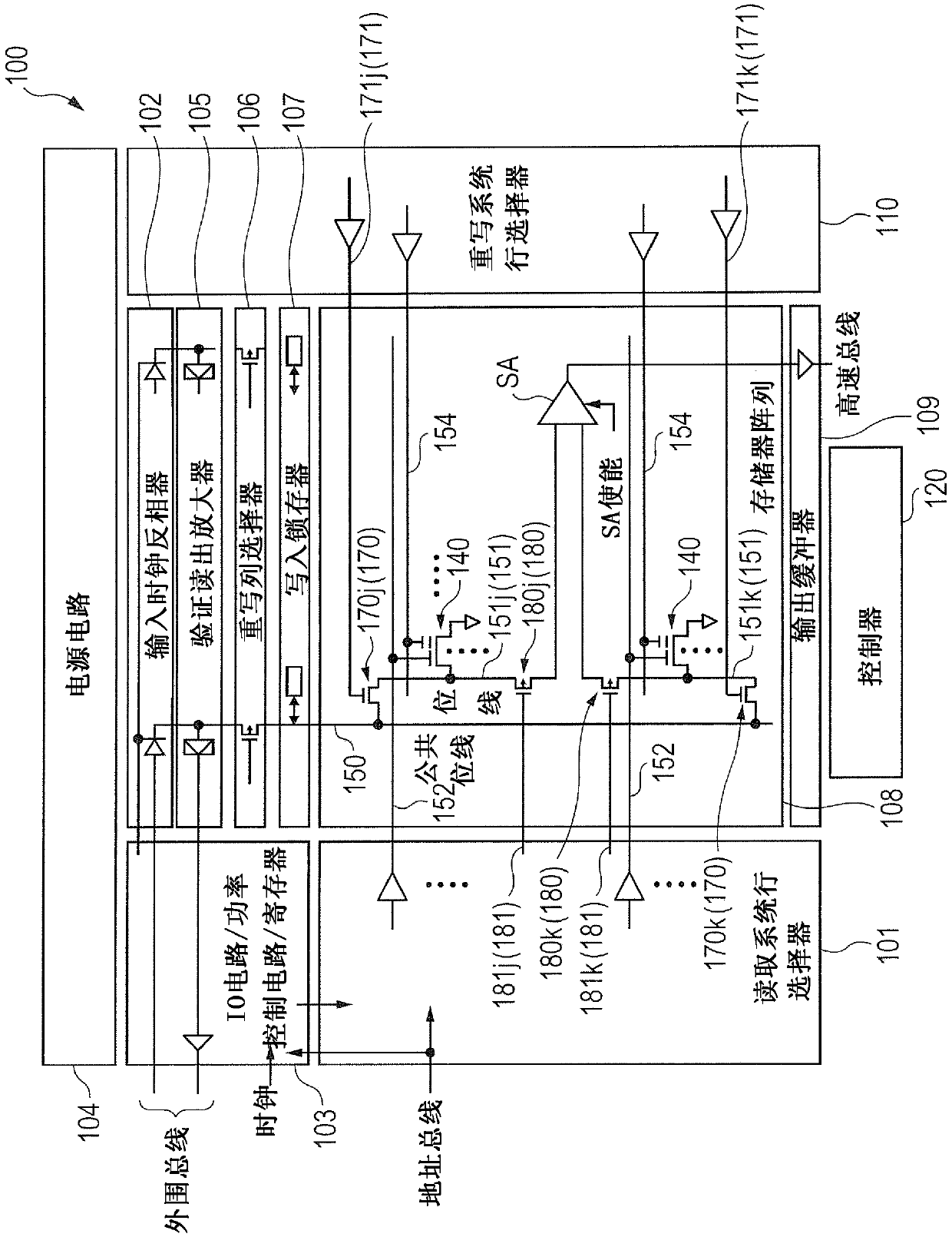
[0182] Figure 16 A diagram showing an example of the structure of a flash memory according to Embodiment 3 of the present invention. Figure 17 An example of the circuit configuration of the sense amplifier and its periphery is shown. Such as Figure 16 As shown, the flash memory 100A is typically composed of the following: read system row selector 101, input clock inverter 102, IO circuit / power control circuit / register 103, power supply circuit 104, verification sense amplifier 105, reset Write column selector 106 , write latch 107 , memory array 108A, output buffer 109 , rewrite system row selector 110 and controller 120 .
[0183] In the flash...
PUM
 Abstract
Description
Claims
Application Information
 - R&D
- Intellectual Property
- Life Sciences
- Materials
- Tech Scout
- Unparalleled Data Quality
- Higher Quality Content
- 60% Fewer Hallucinations
Browse by: Latest US Patents, China's latest patents, Technical Efficacy Thesaurus, Application Domain, Technology Topic, Popular Technical Reports.
© 2025 PatSnap. All rights reserved.Legal|Privacy policy|Modern Slavery Act Transparency Statement|Sitemap|About US| Contact US: help@patsnap.com