
Optical system of a projection exposure equipment for microlithography

An optical system and microlithography technology, applied in the field of optical systems, can solve problems such as damage to the imaging characteristics of projection exposure equipment, deformation, increase in thermal energy input, etc.

Active Publication Date: 2021-07-20
CARL ZEISS SMT GMBH
View PDF3 Cites 0 Cited by
  • Summary
  • Abstract
  • Description
  • Claims
  • Application Information

AI Technical Summary

Problems solved by technology

[0007] A practical problem associated with increasing the light output of an EUV light source is that partial blocking of the EUV light (which is necessary in some areas within the projection exposure tool due to design) leads to an increase in thermal energy input with light output, which in turn leads to Undesired heat-based deformation of EUV mirrors (and possibly mirror holding devices)
[0008] These deformations in turn lead to impairment of the imaging properties of the projection exposure equipment

Method used


Image

  • Optical system of a projection exposure equipment for microlithography
  • Optical system of a projection exposure equipment for microlithography
  • Optical system of a projection exposure equipment for microlithography

Examples


Embodiment Construction

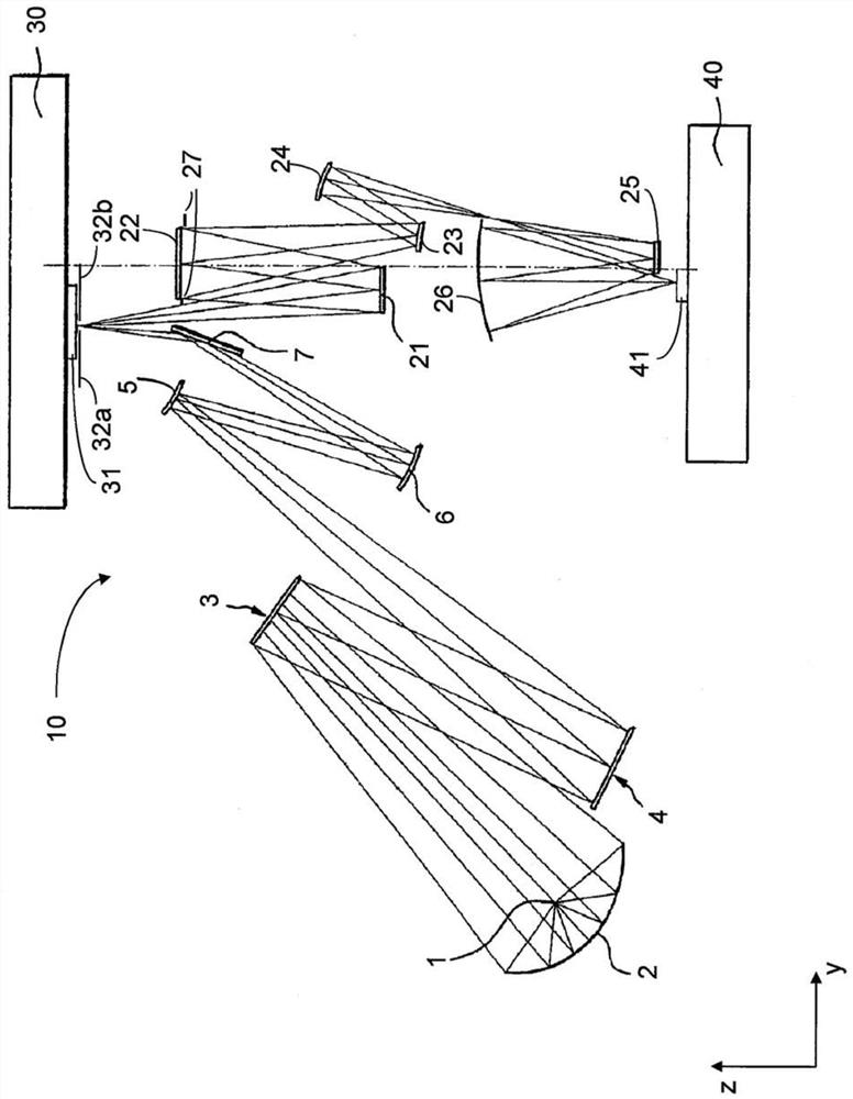
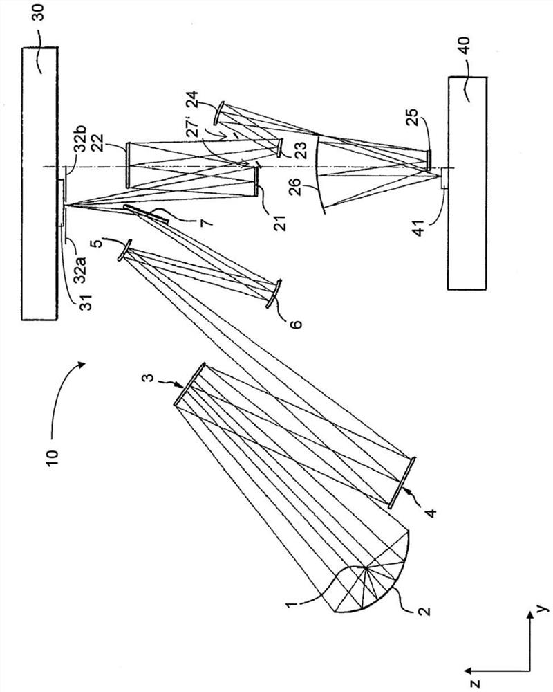
[0038] first, Figure 1a A schematic diagram of a projection exposure apparatus 10 is shown, which is given by way of example and is designed for operation in the EUV range.

[0039] according to Figure 1a, the illumination device of the projection exposure apparatus 10 includes a field facet mirror 3 and a pupil facet mirror 4 . Light comes from a light source unit comprising, for example, a plasma light source 1 and a collector mirror 2 , directing the light onto a field facet mirror 3 . A first telescopic mirror 5 and a second telescopic mirror 6 are arranged in the optical path downstream of the pupil facet mirror 4 . A deflecting mirror 7 is arranged downstream in the beam path, which deflecting mirror directs the radiation incident thereon onto the object field in the object plane of a projection lens comprising six mirrors 21-26. At the position of the object field, a reflective structure-bearing mask 31 is arranged on a mask table 30, said mask being imaged by means ...


PUM


Abstract

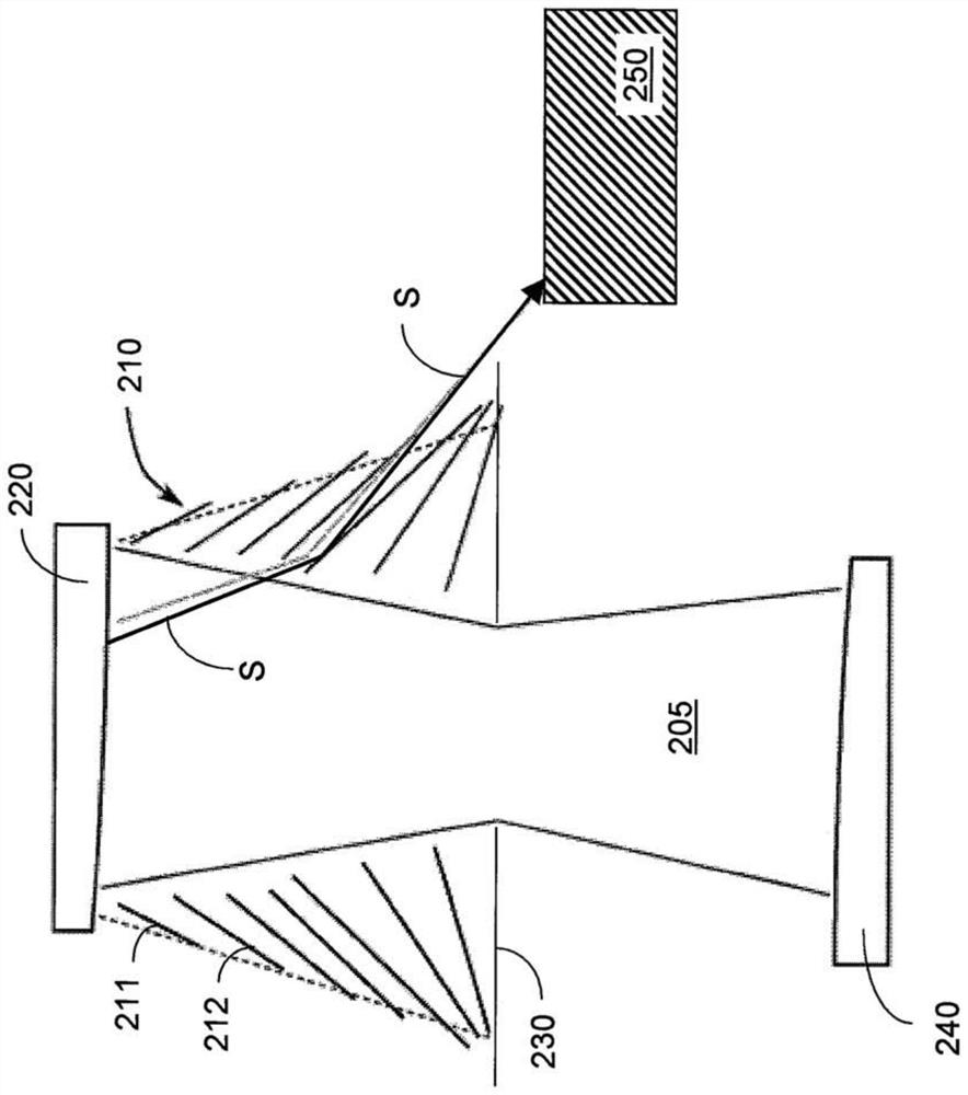
The invention relates to an optical system of a projection exposure apparatus for microlithography, wherein said projection exposure apparatus has an illumination unit and a projection objective, and wherein the light is present during operation of the projection exposure apparatus using light pipes (205, 305) Light in the illumination unit travels from the entrance of the illumination unit via the object plane of the projection objective to the image plane of the projection objective, the optical system having at least one thin layer assembly (210, 310, 410, 420, 430, 440, 450, 510, 520 , 610), the thin layer assembly has at least one reflective thin layer (211,212,311,312,511,512,611,612), and has at least one beam dump (250), wherein the thin layer assembly ( 210 , 310 , 410 , 420 , 430 , 440 , 450 , 510 , 520 , 610 ) are arranged such that during operation of the projection exposure apparatus, light will be at least periodically shone on the thin layer assembly and not part of the use of light pipes ( 205, 305) is reflected towards the beam dump (250).

Description

[0001] Cross References to Related Applications [0002] This application claims priority from German patent application DE 10 2015 210 041.3 filed on June 1, 2015. The content of this German application is incorporated by reference in the text of the present application. technical field [0003] The invention relates to an optical system of a projection exposure device for microlithography. Background technique [0004] Microlithography is used to manufacture microstructured components, such as integrated circuits or LCDs. The microlithography process is carried out in a so-called projection exposure apparatus, which consists of an illumination device and a projection lens. The image of the mask (=reticle) illuminated by the illumination device is in this case projected by a projection lens onto a substrate (e.g. a silicon wafer) coated with a photosensitive layer (photoresist) and arranged on the image plane of the projection lens ), thereby transferring the mask struct...

Claims


Application Information

Patent Timeline
IPC IPC(8): G03F7/20
CPCG03F7/70066G03F7/70075G03F7/702G03F7/70891
Inventor M.帕特拉
Owner CARL ZEISS SMT GMBH
Learn More