Source-drain resistance-variable type H-shaped grid-controlled bidirectional switching transistor and manufacturing method thereof

A bidirectional switch and transistor technology, applied in semiconductor/solid-state device manufacturing, semiconductor devices, electrical components, etc., can solve the problem of device switching performance degradation, loss of control of the gate, and reduced control ability of the gate electrode to the drain and source regions, etc. question

Active Publication Date: 2018-03-20
宿松新驱光电科技有限公司
View PDF2 Cites 4 Cited by
  • Summary
  • Abstract
  • Description
  • Claims
  • Application Information

AI Technical Summary

Problems solved by technology

However, in order to realize the switching characteristics of the gate electrode of the usual Schottky barrier field effect transistor (the gate electrode is forward-conducting and reverse-blocking or reverse-conducting and forward-blocking), it is necessary to perform a specific conductivity type on the source or drain region of the device. impurity doping, which makes it difficult to achieve a good Schottky contact between the source electrode and the source region, between the drain electrode and the drain region, and the doping of the source region and the drain region makes the gate electrode to the drain The control ability of the region and the source region is reduced, resulting in a decrease in the switching performance of the device
If the semiconductor region of the device is not doped, it is easy to realize the Schottky barrier between the source electrode and the source region, and the drain electrode and the drain region in the process, but this will cause the device to have different types in the forward and reverse directions. The carrier conduction of the gate electrode, that is, both the forward bias and reverse bias of the gate electrode will make the device in the conduction state, so that the gate loses its control function as the device switching device

Method used


Image

  • Source-drain resistance-variable type H-shaped grid-controlled bidirectional switching transistor and manufacturing method thereof
  • Source-drain resistance-variable type H-shaped grid-controlled bidirectional switching transistor and manufacturing method thereof
  • Source-drain resistance-variable type H-shaped grid-controlled bidirectional switching transistor and manufacturing method thereof

Examples


Embodiment Construction

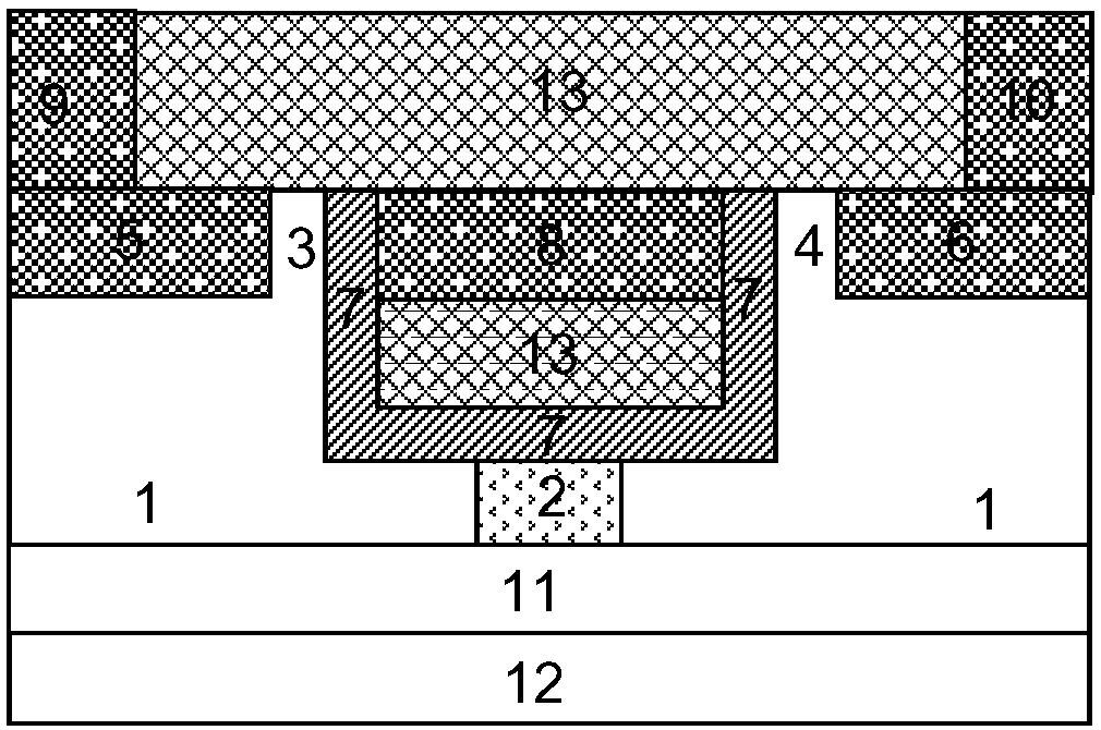
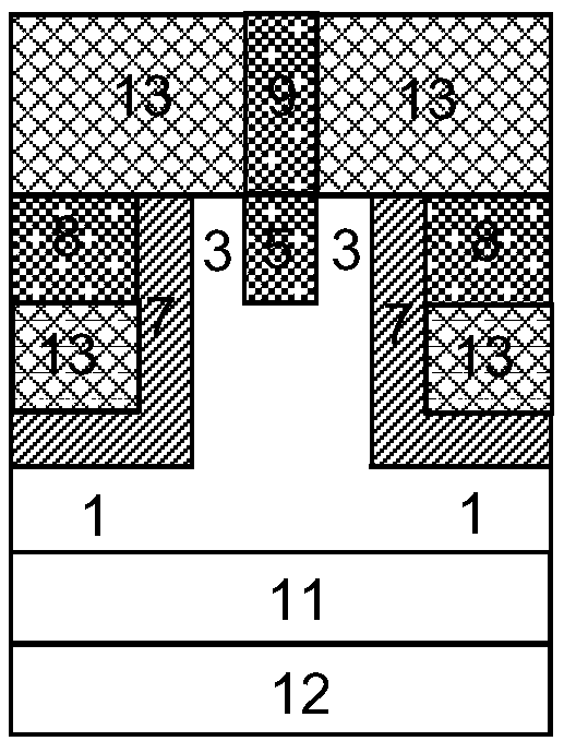
[0072] Below in conjunction with accompanying drawing, the present invention will be further described:

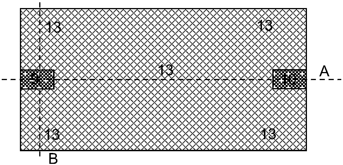
[0073] Such as figure 1 , figure 2 and image 3 As shown, a source-drain resistance variable H-shaped gate-controlled bidirectional switch transistor includes a silicon substrate 12 of an SOI wafer, and the silicon substrate 12 of the SOI wafer is a substrate insulating layer 11 of the SOI wafer. Above the round substrate insulating layer 11 is a monocrystalline silicon film 1 and a heavily doped region 2; 16 cm -3 single crystal silicon semiconductor material; the heavily doped region 2 is located in the middle region of the bottom horizontal part of the single crystal silicon thin film 1 U-shaped structure, the conductivity type of the doped impurities determines the conduction type of the device, and its interior is not affected by the H-shaped gate electrode 8 field effect influence control, the impurity concentration is not less than 10 17 cm -3 The semiconduct...


PUM


Abstract

The invention relates to a source-drain resistance-variable type H-shaped grid-controlled bidirectional switching transistor and a manufacturing method thereof. According to the invention, the transistor comprises an H-shaped grid electrode and structural features which are symmetric on the left side and the right side. The transistor is strong in grid control capability, and a metal source / draininterchangeable region can be controlled as a source region or a drain region through adjusting the electrode voltage of the source / drain interchangeable region. In this way, the direction of the tunneling current is changed. The invention has the advantages of low static power consumption, reverse leakage current, strong grid control capability, low sub-threshold swing and bidirectional switchingfunction. Compared with a common MOSFETs-type device, more excellent switching characteristics are achieved through the tunneling effect. Compared with a common tunneling field effect transistor, better switching characteristics are realized compared with a Schottky barrier transistor. Meanwhile, the doping is not needed in the source and drain regions, and the Schottky barrier is easy to form. The H-shaped grid electrode can better control the source and drain regions. Therefore, the transistor is suitable for popularization and application.

Description

technical field [0001] The invention relates to the field of ultra-large-scale integrated circuit manufacturing, in particular to a source-drain resistance variable H-shaped gate-controlled bidirectional switch transistor with low leakage current suitable for low-power integrated circuit manufacturing and a manufacturing method thereof. Background technique [0002] According to the requirements of Moore's law, MOSFETs, the basic unit of integrated circuits, must become smaller and smaller in size. The resulting problem is not only the increase in the difficulty of the manufacturing process, but also the adverse effects of the device itself caused by the smaller size. highlight. Due to the limitation of the physical mechanism of current generation of MOSFETs used in integrated circuit design, the subthreshold swing cannot be lower than 60mV / dec. [0003] When ordinary tunneling field effect transistors are used as switching devices, the tunneling mechanism of carriers is us...

Claims


Application Information

Patent Timeline
Patent Type & Authority Applications(China)
IPC IPC(8): H01L29/08H01L29/423H01L29/78H01L21/336H01L21/28
Inventor 靳晓诗高云翔刘溪
Owner 宿松新驱光电科技有限公司
Why Eureka
Try Eureka