
Preparation method of Micro-LED light emitting display device

A light-emitting display device and device technology, which is applied in the manufacture of semiconductor/solid-state devices, electric solid-state devices, semiconductor devices, etc., can solve the problems of reducing the size of soldered chips, prone to false soldering, and low yield rate, and achieves reduction in soldering size, Efficiency and yield rate improvement, the effect of high yield rate

Active Publication Date: 2018-04-06
FUZHOU UNIVERSITY
View PDF3 Cites 23 Cited by
  • Summary
  • Abstract
  • Description
  • Claims
  • Application Information

AI Technical Summary

Problems solved by technology

[0003] The existing traditional metal ball welding is to prepare metal balls at specific positions on the LED chip and CMOS backplane, and then align and weld them together. After the metal electrode material is made on the chip, the metal electrode material at other positions is removed by photolithography and other means. A high-precision alignment system is required, and it is difficult to further reduce the size of the soldered chip. The equipment is expensive, low in efficiency, and prone to false soldering. , resulting in low yield

Method used


Image

  • Preparation method of Micro-LED light emitting display device
  • Preparation method of Micro-LED light emitting display device
  • Preparation method of Micro-LED light emitting display device

Examples


preparation example Construction

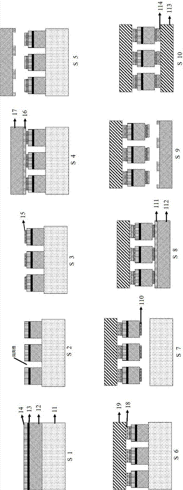
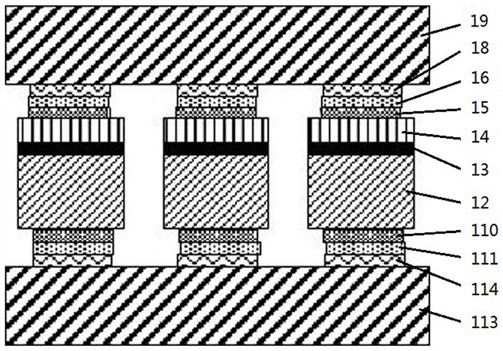
[0031] like figure 1 As shown, a method for preparing a Micro-LED light-emitting display device includes:

[0032] S1: Deposit an n-type GaN epitaxial layer 12, a multi-quantum well layer 13, and a p-type GaN epitaxial layer 14 on the clean GaN substrate 11 from bottom to top;

[0033] S2: Use photolithography and etching to form isolation grooves on the deposited n-type GaN epitaxial layer 12, multi-quantum well layer 13 and p-type GaN epitaxial layer 14 to form a Micro-LED unit device array containing multiple unit devices ;

[0034] S3: making a p-type ohmic contact layer 15 on the p-type GaN epitaxial layer 14 of each unit device in the Micro-LED unit device array;

[0035] S4: Evenly coat a layer of conductive paste on the surface of a clean first template 17, and place the p-type ohmic contact layer 15 of the Micro-LED unit device array on the conductive paste, that is, the conductive paste of the first template 17 The paste is in contact with the p-type ohmic contact...


PUM


Abstract

The invention relates to a preparation method of a Micro-LED light emitting display device. The preparation method comprises the steps of preparing a GaN-based epitaxial layer firstly; next, forming aMicro-LED unit device array by adopting a chip process; next, manufacturing an ohmic contact layer, and enabling the Micro-LED unit device array to be connected on a CMOS or a TFT back plate througha micro contact printing mode; and finally, adopting a laser lift-off mode, realizing lift-off between the epitaxial layer and the GaN substrate, and enabling the Micro-LED unit device array to be connected to another substrate through metal welding, bonding or micro contact printing mode, so as to form the Micro-LED light emitting display device. Compared with the prior art, the preparation method is simple in process, high in yield and low in cost; and in addition, the Micro-LED light emitting display device can be prepared on glass, a silicon substrate or even a polymer flexible substrate.

Description

technical field [0001] The invention relates to the field of novel semiconductor displays, in particular to a method for preparing a Micro-LED light-emitting display device. Background technique [0002] Micro-LED is a display technology that miniaturizes and matrixes the traditional LED structure, and uses CMOS integrated circuit technology to make a driving circuit to realize the addressing control and individual driving of each pixel. Since the brightness, life, contrast, response time, energy consumption, viewing angle and resolution of Micro-LED technology are stronger than those of LCD and OLED technology, plus it is self-illuminating, simple in structure, small in size and energy-saving. The advantages of the display technology have been regarded as the next generation of display technology by many manufacturers and have begun to actively lay out. In the preparation process of Micro-LEDs, in order to continuously improve the performance of Micro-LEDs such as resoluti...

Claims


Application Information

Patent Timeline
IPC IPC(8): H01L21/82H01L27/15H01L33/36
CPCH01L21/82H01L27/156H01L33/36H01L2933/0016
Inventor 周雄图张永爱严群郭太良林金堂叶芸翁雅恋
Owner FUZHOU UNIVERSITY
Learn More