Array substrate, manufacturing method of array substrate, display panel and manufacturing method of display panel

A technology of an array substrate and a manufacturing method, which is applied in the display field and can solve problems such as low printing resolution and high difficulty of printing process

Active Publication Date: 2018-04-10
BOE TECH GRP CO LTD
View PDF3 Cites 17 Cited by
  • Summary
  • Abstract
  • Description
  • Claims
  • Application Information

AI Technical Summary

Problems solved by technology

[0005] The invention provides an array substrate and a manufacturing method thereof, a display panel and a manufacturing method thereo

Method used


Image

  • Array substrate, manufacturing method of array substrate, display panel and manufacturing method of display panel
  • Array substrate, manufacturing method of array substrate, display panel and manufacturing method of display panel
  • Array substrate, manufacturing method of array substrate, display panel and manufacturing method of display panel

Examples


Embodiment 1

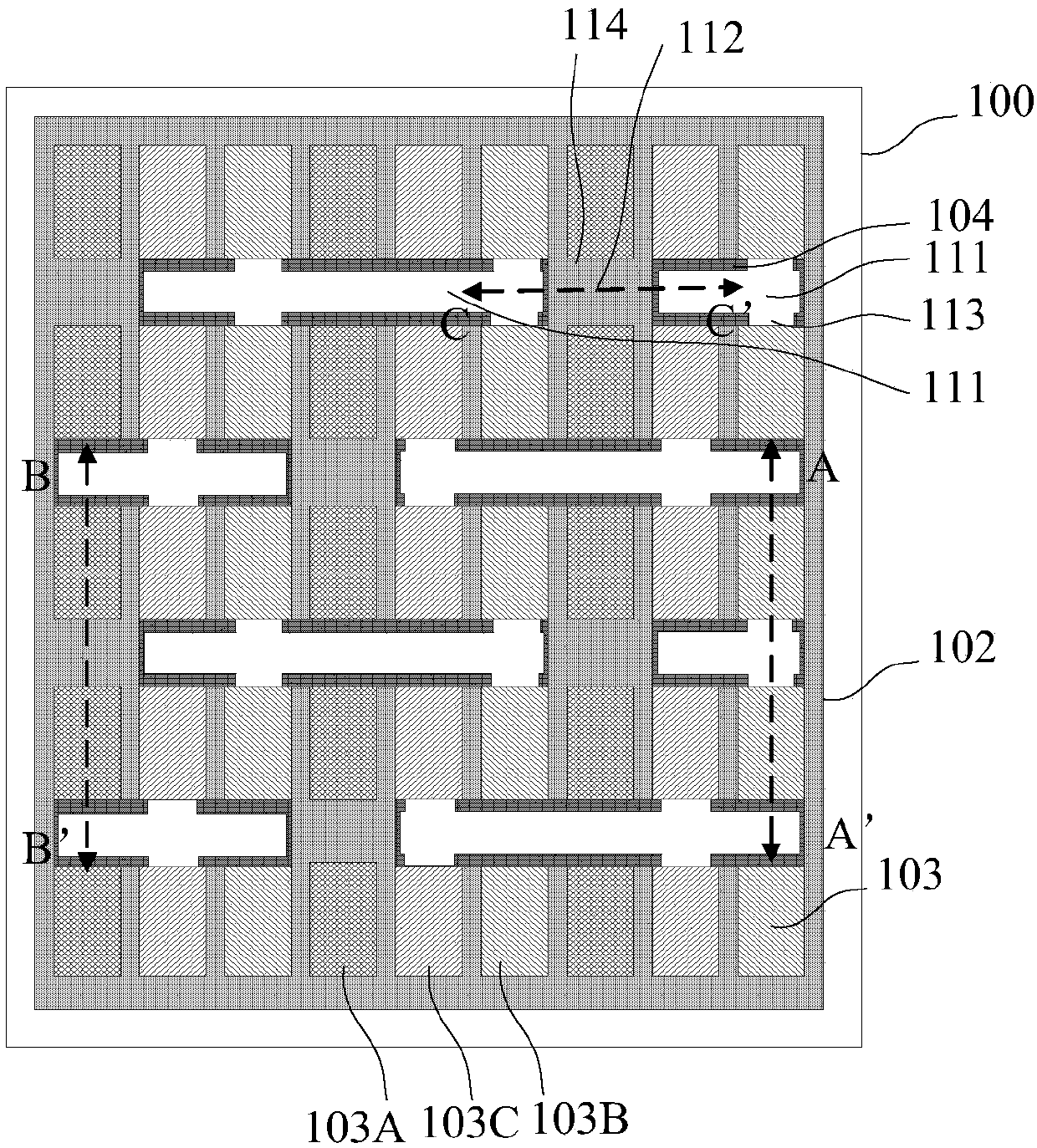
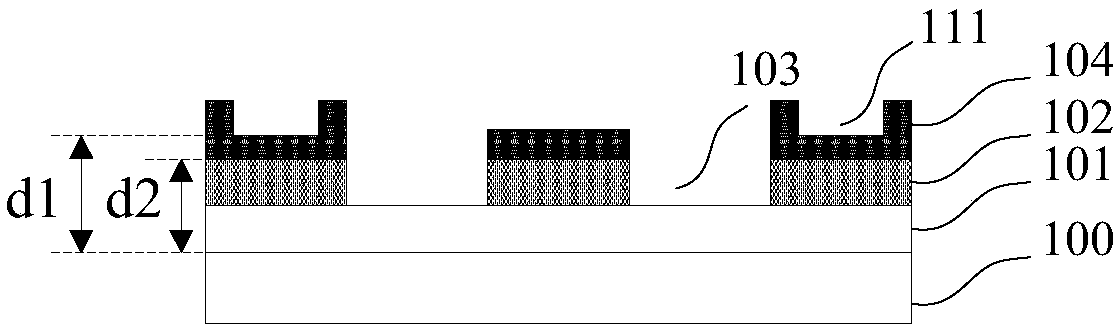
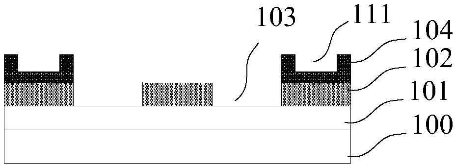
[0046] figure 1 is a schematic structural diagram of an array substrate according to an embodiment of the present invention, figure 2 for figure 1 The partial sectional view of the array substrate shown along section A-A', image 3 for figure 1 The partial cross-sectional view of the array substrate shown along section B-B'.

[0047] combine figure 1 , figure 2 with image 3 As shown, the embodiment of the present invention provides an array substrate, including: a base substrate 100, an electrode layer 101 formed on the base substrate 100, and a first pixel defining layer 102. The first pixel defining layer 102 connects the base substrate 100 is divided into a plurality of sub-pixel regions 103; a second pixel-defining layer 104 is formed on the first pixel-defining layer 102 between at least two adjacent rows of sub-pixel regions 103, and the second pixel-defining layer 104 is provided with multiple a first groove 111, a second groove 112 is arranged between two adjac...

Embodiment 2

[0083] The embodiment of the present invention also provides a display panel, the display panel includes Figure 1 to Figure 6 Either one of the array substrates shown.

[0084] For the specific description of the array substrate, reference may be made to the description of Embodiment 1, which will not be repeated in this embodiment of the present invention.

[0085] In the embodiment of the present invention, the display panel further includes a light-emitting layer formed in the sub-pixel region 103. By inkjet printing, the first light-emitting layer is formed in the sub-pixel region 103A of the first color, and the sub-pixel of the second color A second light-emitting layer is formed in the region 103B, and a third light-emitting layer is formed in the sub-pixel region 103C of the third color.

[0086] In an embodiment of the present invention, the display panel includes an array substrate, adopts a double-layer pixel defining layer structure, and forms a second pixel defi...

Embodiment 3

[0088] refer to Figure 7 , which shows a flow chart of a method for manufacturing an array substrate according to an embodiment of the present invention, which may specifically include the following steps:

[0089] Step 701, forming an electrode layer on a base substrate.

[0090] In the embodiment of the present invention, the electrode layer 101 is formed on the base substrate 100 .

[0091] Wherein, the electrode layer 101 is generally an anode layer, and its material is ITO (Indium Tin Oxide, indium tin oxide); the base substrate 100 can be a glass substrate, a quartz substrate, a metal substrate, a resin substrate, and the like.

[0092] Step 702, forming a first pixel defining layer on the electrode layer.

[0093] In the embodiment of the present invention, the first pixel defining layer 102 is formed on the electrode layer 101 through a patterning process.

[0094] Specifically, a first pixel defining layer film is first deposited on the electrode layer 101 , and a...


PUM

PropertyMeasurementUnit
Thicknessaaaaaaaaaa

Abstract

The invention provides an array substrate, a manufacturing method of the array substrate, a display panel and a manufacturing method of the display panel, and relates to the technical field of display. A second pixel defining layer is formed on a first pixel defining layer between two adjacent rows of sub-pixel areas, a plurality of first grooves are formed in the second pixel defining layer, andsecond grooves are formed between every two adjacent first grooves, a first opening is formed in one side, adjacent to the sub-pixel areas, of the first grooves, and a second opening is formed in oneside, adjacent to the sub-pixel areas, of the second grooves. When a light-emitting layer is subsequently printed, the light-emitting material is directly dripped into the first grooves, the first opening can enable the light-emitting material to flow into the sub-pixel areas communicated with the first grooves, and a luminescent material can also be dripped into the second grooves, and flows intothe sub-pixel areas communicated with the second grooves through the second opening. The structure of the pixel defining layers is changed, the printing resolution is improved on the premise that theexisting equipment is not changed, and the difficulty of the printing process is reduced.

Description

technical field [0001] The present invention relates to the field of display technology, in particular to an array substrate and a manufacturing method thereof, a display panel and a manufacturing method thereof. Background technique [0002] OLED (Organic Light Emitting Diode, organic electroluminescent device) has many advantages such as active light emission, high brightness, high contrast, ultra-thin, low power consumption, flexibility and wide operating temperature range, and has become a very competitive and developing Prospects for next-generation display technologies. [0003] At present, there are two methods of manufacturing OLED display panels. The first method is the evaporation method. The evaporation method can realize the production of OLED full-color products, and can correspond to extremely high resolution, but the material utilization rate is low, and large-size displays The panel should be produced by white light plus color film; the second is inkjet prin...

Claims


Application Information

Patent Timeline
IPC IPC(8): H01L27/32H01L51/56
CPCH10K59/35H10K59/122H10K71/135H10K71/00
Inventor 赵德江刘文祺
Owner BOE TECH GRP CO LTD
Why Eureka
Try Eureka