Preparation method of semiconductor laser material
A semiconductor and laser technology, which is applied in the field of semiconductor laser material preparation, can solve problems such as troubles, adding impurity particles in multiple processes, and achieve the effects of improving crystal quality, eliminating substrate thinning steps, and simplifying the method.
- Summary
- Abstract
- Description
- Claims
- Application Information
AI Technical Summary
Problems solved by technology
Method used
Image

Examples
Embodiment 1
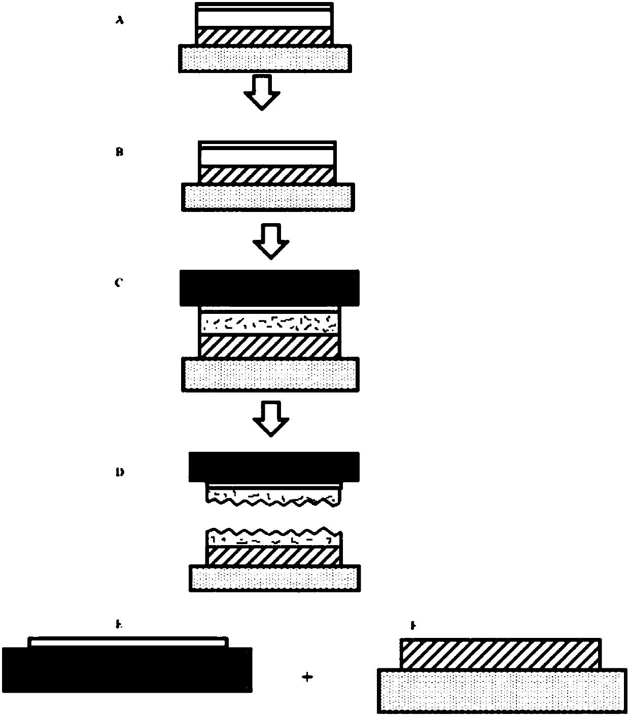
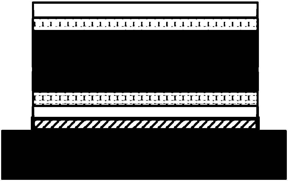
[0034] Taking GaSb and silicon-based substrate heterogeneously integrated growth semiconductor laser process as an example, the process steps of using easily oxidized aluminum-containing compounds in the air as sacrificial layers to realize the reuse of donor substrates are described below. These structures and preparation steps can be directly Extended to other types of semiconductor laser technology, its specific structure can be as follows figure 2 shown. The specific process steps are as follows:
[0035](1) growing a 550nm GaSb buffer layer on the GaSb substrate;
[0036] (2) growing a 600nm AlSb sacrificial layer on the buffer layer;
[0037] (3) grow 200nm n-type doping on the sacrificial layer (the doping concentration of Te is 5×10 18 cm -3 ) GaSb film layer; see figure 1 A, the structure formed at this time is an n-type doped GaSb film capping layer, an AlSb sacrificial layer, a GaSb buffer layer and a GaSb substrate (donor substrate) from top to bottom;
[00...
Embodiment 2
[0049] In this embodiment, except that the substrate is GaAs, the semiconductor thin film layer is GaAs, and the sacrificial layer is AlAs, the rest is a common laser structure on a GaAs substrate, and the method is consistent with Embodiment 1.
Embodiment 3
[0051] In this embodiment, except that the substrate is InP, the semiconductor film layer is InP, and the sacrificial layer is InAlAs, the rest is a common laser structure on an InP substrate, and the method is consistent with Embodiment 1.
PUM
 Abstract
Description
Claims
Application Information
 - R&D
- Intellectual Property
- Life Sciences
- Materials
- Tech Scout
- Unparalleled Data Quality
- Higher Quality Content
- 60% Fewer Hallucinations
Browse by: Latest US Patents, China's latest patents, Technical Efficacy Thesaurus, Application Domain, Technology Topic, Popular Technical Reports.
© 2025 PatSnap. All rights reserved.Legal|Privacy policy|Modern Slavery Act Transparency Statement|Sitemap|About US| Contact US: help@patsnap.com