Measurement method for three-dimensional memory channel conductivity

A measurement method and memory technology, applied in the direction of measuring electricity, measuring devices, measuring electrical variables, etc., can solve problems such as failure of peripheral control circuits, immature technology, and open circuit of control gate circuits.

Active Publication Date: 2018-05-04
YANGTZE MEMORY TECH CO LTD
View PDF9 Cites 2 Cited by
  • Summary
  • Abstract
  • Description
  • Claims
  • Application Information

AI Technical Summary

Problems solved by technology

In evaluating the integrity of the channel, in addition to the slice analysis of the physical structure of the channel, it is also necessary to test the conductivity of the channel to obtain the electrical parameters of the channel. However, due to the immature technology and unstable process in the research and development stage There are various defects in the trial-produced chips, such as control gate circuit open circuit, short circuit, source leakage, etc., in order to obtain the conductivity parameters of the channel hole in advance and avoid the process of the peripheral circuit from improving the progress of the channel process. Therefore, it is necessary to design a new method to quickly realize the measurement of the electrical characteristics of the channel itself.
[0004] It can be seen that the traditional measurement of the channel electrical characteristics of a three-dimensional memory chip has the following problems: first, it needs to be carried out after the peripheral control circuit pro

Method used


Image

  • Measurement method for three-dimensional memory channel conductivity
  • Measurement method for three-dimensional memory channel conductivity
  • Measurement method for three-dimensional memory channel conductivity

Examples


Embodiment

[0033] A method for measuring the conductivity of a three-dimensional memory channel, comprising the following steps:

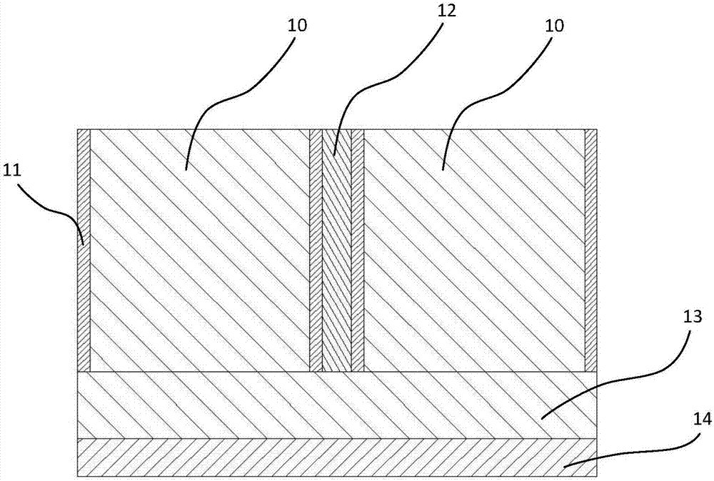
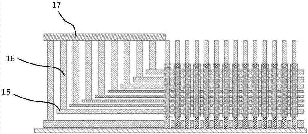
[0034] The step of preparing the three-dimensional memory sample to be tested, the step includes, such as figure 2 As shown, the upper surface of the three-dimensional memory is ground until the tungsten plug layer 16 of the three-dimensional memory is exposed. Specifically, the grinding process can be a chemical mechanical grinding method. After the grinding process, the sample surface is cleaned to Keep the surface of the sample to be tested clean, and use a heating platform to bake the sample to be tested to remove the residual moisture on the sample to be tested;

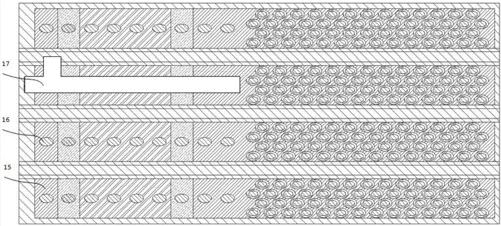
[0035] The step of selecting the test object is to judge the connection state between the tungsten plug exposed in the array step area of ​​the three-dimensional memory and the word line layer according to the voltage contrast method VC (voltage contrast). The line layer is well connected, an...


PUM


Abstract

The invention provides a measurement method for three-dimensional memory channel conductivity. Through combing a focusing ion beam machine and a nano-point needle table, the accuracy of the channel conductivity can be tested in advance before improving a peripheral circuit technique. The influence of poor problems of the peripheral control circuit on the three-dimensional memory channel conductivity in a traditional measurement method is solved, the test of the channel conductivity itself is realized, and the technical research and development cycle is shortened.

Description

technical field [0001] The invention relates to the field of testing the performance of semiconductor devices, in particular to a testing method for the continuity of a three-dimensional memory channel. Background technique [0002] Three-dimensional memory (3D NAND) is an emerging memory type that solves the limitations of 2D or planar NAND flash memory by stacking memory particles together. Instead of placing memory chips on a single side, the new 3D NAND technology stacks multiple layers of data storage cells vertically. Based on this technology, storage devices with a storage capacity several times higher than similar NAND technologies can be created. The technology enables higher storage capacity in a smaller footprint, resulting in significant cost savings, reduced power consumption, and dramatic performance gains for many consumer mobile devices and the most demanding enterprise deployments demand. [0003] In the design and development stage of a three-dimensional...

Claims


Application Information

Patent Timeline
IPC IPC(8): G01R31/28
CPCG01R31/2853
Inventor 鲁柳张顺勇汤光敏刘刚
Owner YANGTZE MEMORY TECH CO LTD
Why Eureka
Try Eureka