

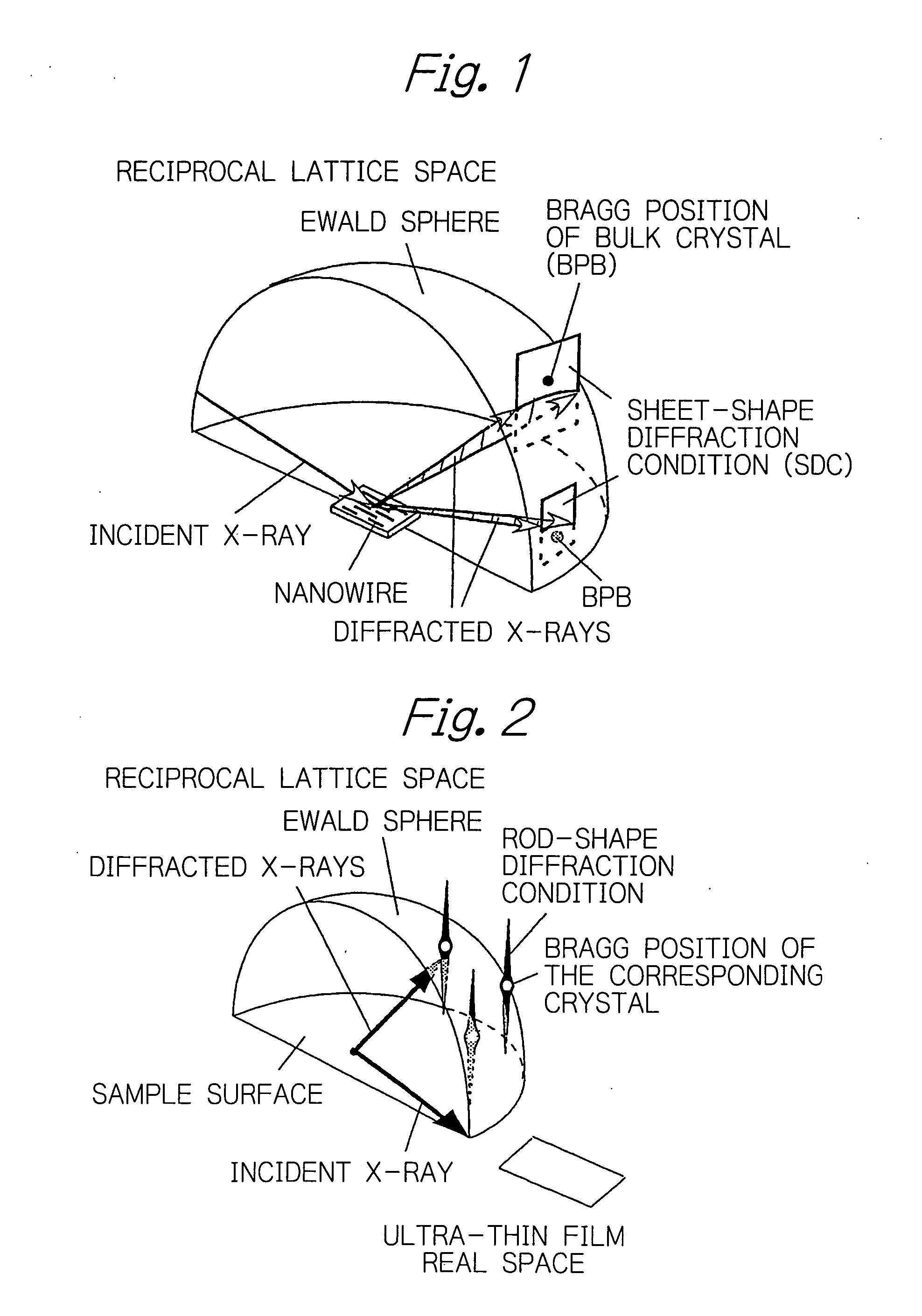
Rapid X-ray diffraction method for structural analysis of a nano material on a surface or at an interface and for structural analysis of a solid/liquid interface, and apparatus used for the method
a nano-material and structural analysis technology, applied in the direction of material analysis using wave/particle radiation, polycrystalline material growth, instruments, etc., can solve the problems of difficult to obtain the overall image of the diffraction intensity profile, the inability to obtain information about the buried ultra-fine structure by spm, and the comparatively long time of measurement. achieve the effect of reducing the cost of development, efficient relationship between the functions of these devices and their structures at a nano-scale, and rapid
- Summary
- Abstract
- Description
- Claims
- Application Information
AI Technical Summary
Benefits of technology
Problems solved by technology
Method used
Image

Examples
example 1
[0079] Case 1 of Ultra-Fine Nanowires Grown on a Substrate Crystal Surface (Method of Rapid X-Ray Structural Analysis of Ultra-Fine Structures)
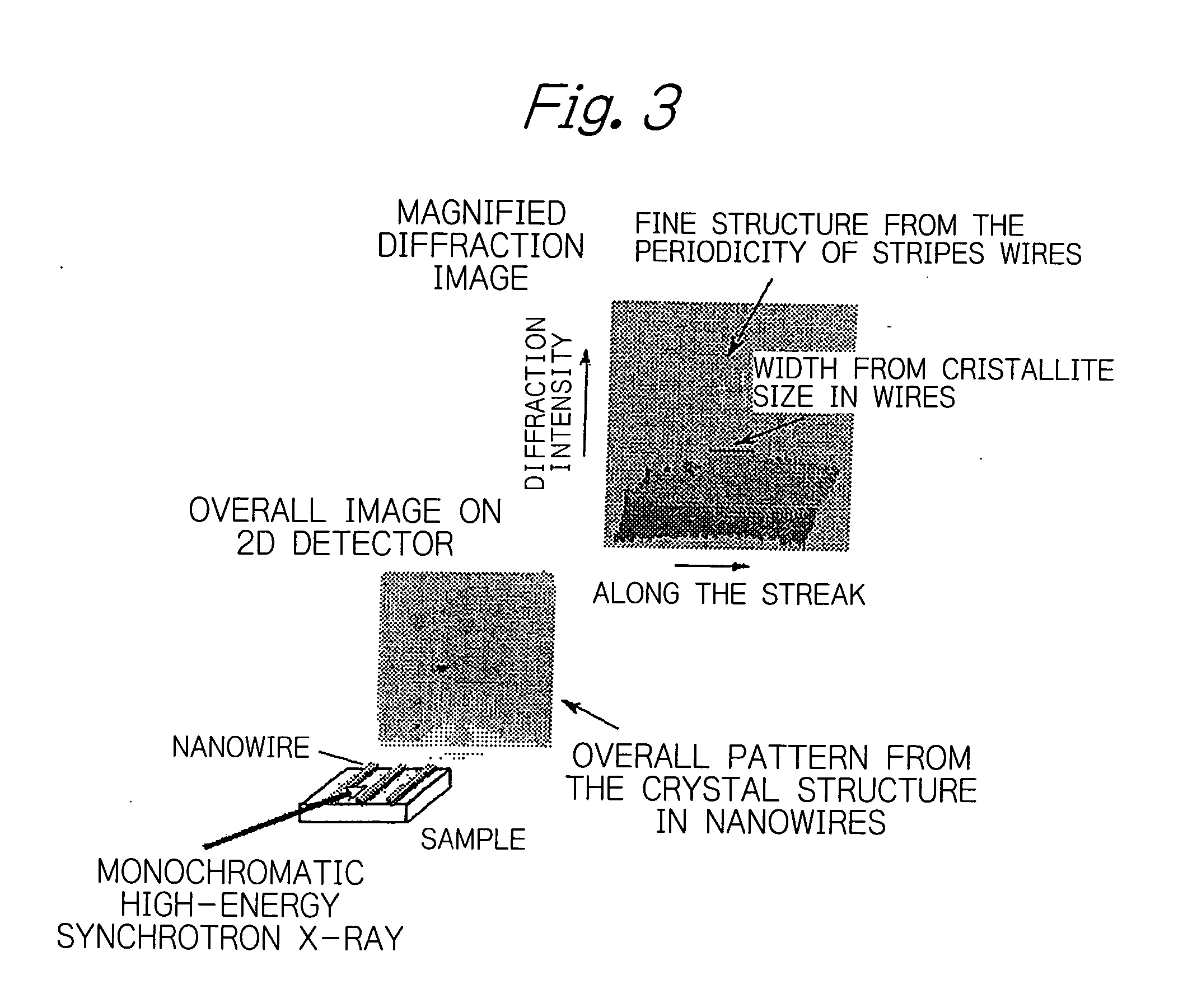
[0080] In this Example, ultra-fine nickel oxide (NiO) nanowires (0.5 nm high) were epitaxially deposited on a sapphire single crystal (0001) and x-rays were incident substantially normal to those nanowires. The incident x-rays had a wavelength of 0.05 nm and formed an angle of 0.05 degrees with the sample surface. An imaging plate as a two-dimensional x-ray detector was set perpendicular to the incident x-rays. The results are shown in FIG. 5.
[0081] From the overall pattern of diffraction images, it was found that the ultra-fine nanowires under test had a hexagonal structure, with the crystal lattice parameters having lengths of 0.476, 0.476 and 0.421 nm and angles of 90, 90 and 120 degrees. It was also found that those nanowires were perpendicular to the [1 0-1 0] direction of the sapphire substrate. From the width of one diffraction image...
example 2
Case 2 of Ultra-Fine Nanowires Grown on a Substrate Crystal Surface (Method of Rapid X-Ray Structural Analysis of Ultra-Fine Structures)
[0082] In this Example, ultra-fine nickel oxide (NiO) nanowires (0.5 nm high) were deposited on a sapphire single crystal (0001) and x-rays were incident substantially parallel to those nanowires. The sample was prepared under almost the same conditions as in Example 1. The incident x-rays having a wavelength of 0.05 nm formed an angle of 0.2 degrees with the sample surface. An imaging plate as a two-dimensional x-ray detector was set perpendicular to the incident x-rays. The results are shown in FIG. 6.
[0083] From the overall pattern of diffraction images, it was found that the ultra-fine nanowires under test had a hexagonal structure, with the crystal lattice parameters having lengths of 0.476, 0.476 and 0.421 nm and angles of 90, 90 and 120 degrees. It was also found that those nanowires were not completely parallel to, but 5 degrees offset fro...
example 3
Case 1 of Buried Ultra-Fine Nanolines Sandwiched Between a Substrate Crystal and an Overlying Cap Layer (Method of Rapid X-Ray Structural Analysis of Ultra-Fine Structures) (Apparatus for Rapid X-Ray Structural Analysis of Ultra-Fine Structures)
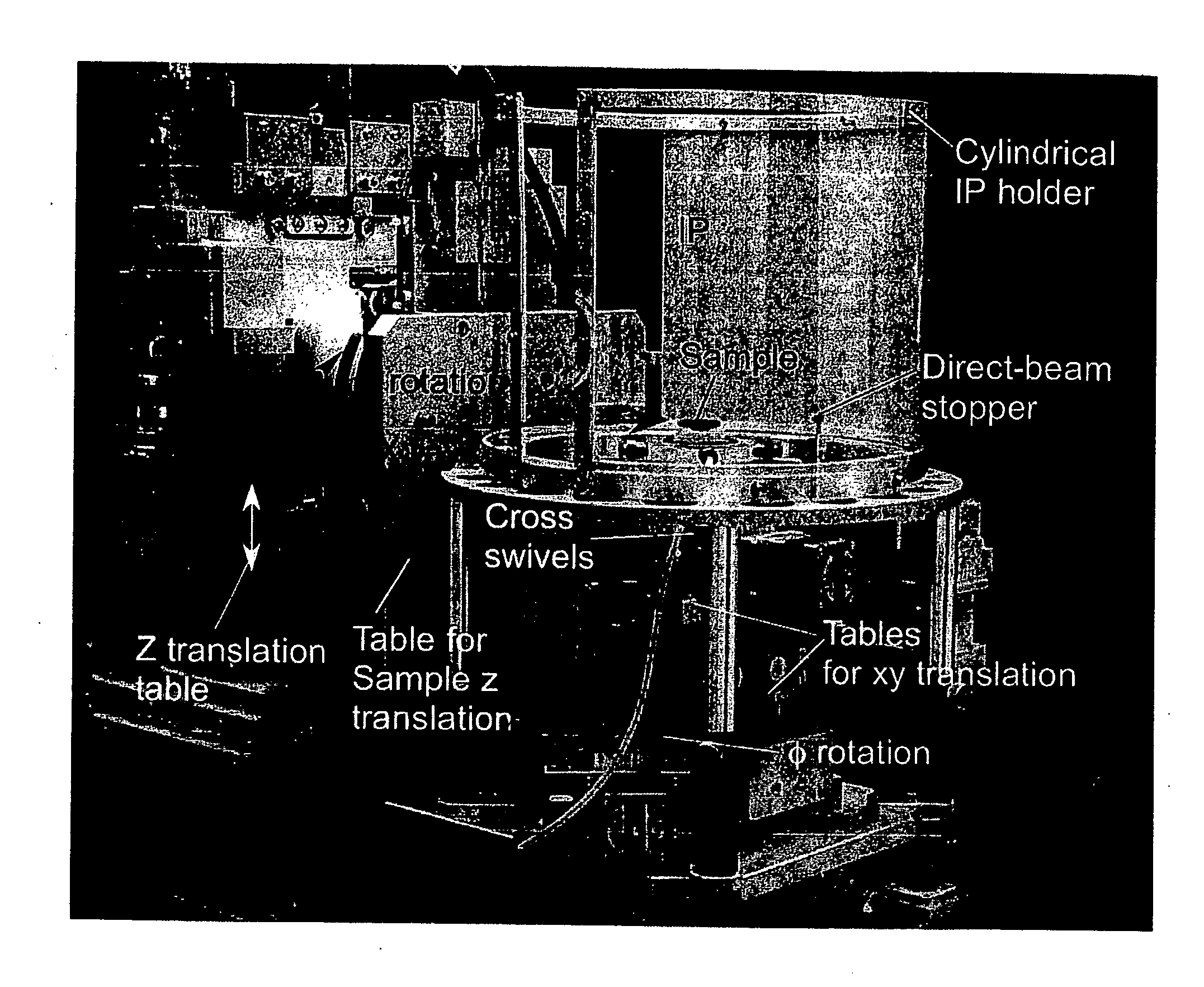
[0085] In this Example, bismuth (Bi) nanolines (monolayer in height, 1.5 nm in width, and ca. 400 nm in length) were grown on a silicon (Si) single-crystal (001) surface, a silicon (Si) cap layer was epitaxially grown in a thickness of about 10 nm over those nanolines, and x-rays were incident normal to the nanolines. The incident x-rays (with a wavelength of 0.05 nm) formed an angle of 0.1 degree with the sample surface. A cylindrical imaging plate as a two-dimensional x-ray detector was installed in such a way that its axis of the cylinder holder was parallel to the vertical axis passing through the sample. The results are shown in FIG. 7. Both the sample and the detector were fixed in angle and position during x-ray exposure. The right-ha...
PUM
| Property | Measurement | Unit |
|---|---|---|
| critical angle | aaaaa | aaaaa |
| size | aaaaa | aaaaa |
| size | aaaaa | aaaaa |
Abstract
Description
Claims
Application Information