Manufacturing method of trench-gate superjunction device

A technology of superjunction device and manufacturing method, which is applied in the manufacture of semiconductor/solid state devices, semiconductor devices, electrical components, etc., can solve the problems of increasing the specific on-resistance of the device, affecting the diffusion of P-type pillars and N-type pillars, etc. The effect of reducing specific on-resistance, reducing leakage, and high doping concentration

Inactive Publication Date: 2018-05-04
SHENZHEN SANRISE TECH CO LTD
View PDF7 Cites 5 Cited by
  • Summary
  • Abstract
  • Description
  • Claims
  • Application Information

AI Technical Summary

Problems solved by technology

In this way, the thermal process during the formation of the trench gate will affect the diffusion between the P-type column and the N-type column, especially when forming a gate oxide layer or forming a sacrificial oxide layer requires a very high temperature. It will intensify the diffusion of P-type impurities to N-type pillars, resulting in an increase in the specific on-resistance of the device

Method used


Image

  • Manufacturing method of trench-gate superjunction device
  • Manufacturing method of trench-gate superjunction device
  • Manufacturing method of trench-gate superjunction device

Examples


Embodiment 1

[0050] Embodiment one method of the present invention:

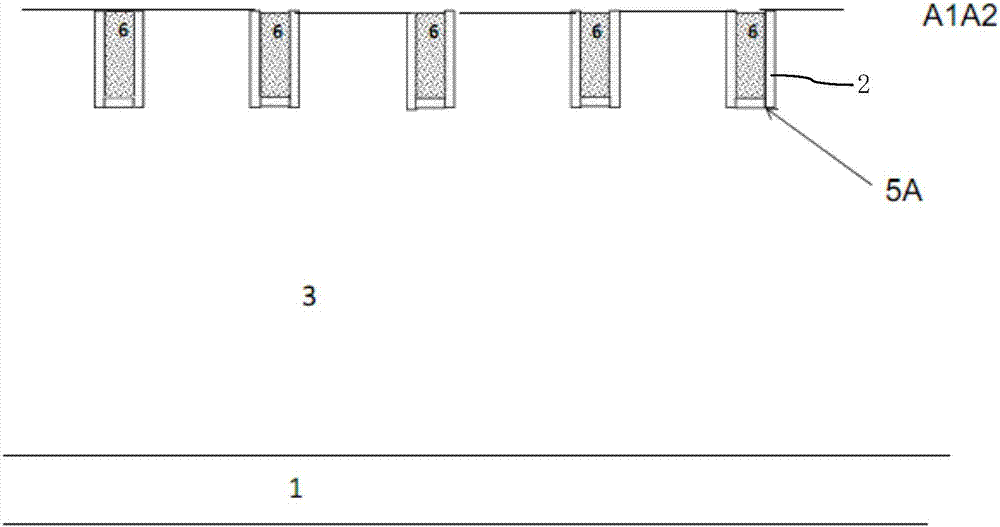
[0051] Such as figure 1 Shown is the flowchart of a method of the embodiment of the present invention; Figure 2 to Figure 7 As shown, it is a schematic diagram of the device structure in each step of the method of the first embodiment of the present invention; the manufacturing method of the trench gate super junction device of the first embodiment of the present invention includes the following steps:

[0052] Step 1, forming the trench gate 6 includes the following sub-steps:

[0053] Step 11, such as figure 2 As shown, the first epitaxial layer 3 of the first conductivity type is provided, and the first epitaxial layer 3 is formed on the surface of the semiconductor substrate 1 of the first conductivity type. The semiconductor substrate 1 in Embodiment 1 of the present invention is a silicon substrate. Bottom, the first epitaxial layer 3 is a silicon epitaxial layer, and the subsequent second epitaxial layer 4 is...

Embodiment 2

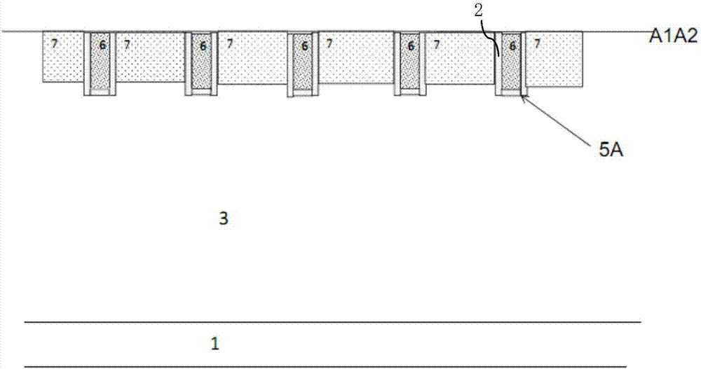
[0089] The second method of the embodiment of the present invention:

[0090] The difference between the second method of the present invention and the first method of the embodiment of the present invention is:

[0091] The step of forming the well region 7 of the second conductivity type is performed after step 2, and the step of forming the well region 7 of the second conductivity type is also performed before the deposition process of the field oxide film. The well region of the second conductivity type The implanted area of ​​region 7 is defined using photolithography. In other embodiments, instead of using photolithography to define the injection region of the second conductivity type well region 7 , the second conductivity type well region 7 can be formed by full-scale implantation.

[0092] After the second conductivity type well region 7 is implanted, a high-temperature push-in well is required. In Embodiment 2 of the present invention, the annealing temperature of t...

Embodiment 3

[0094] Embodiment three methods of the present invention:

[0095] The difference between the method of the third embodiment of the present invention and the method of the first embodiment of the present invention is:

[0096] The step of forming the well region 7 of the second conductivity type is performed after step 2, and the step of forming the well region 7 of the second conductivity type is also performed after the patterning process of the field oxide film. The well region of the second conductivity type The implantation of zone 7 was a global implantation.

[0097] Wherein, the step of forming the pattern structure of the field oxide film includes: depositing the field oxide film first, then forming the pattern of the field oxide film by photolithography and etching, and finally forming the pattern in the terminal area, or the terminal area and The field oxide film of 8000 angstroms to 15000 angstroms is formed in the transition area, while the field oxide film is no...


PUM

PropertyMeasurementUnit
Thicknessaaaaaaaaaa
Thicknessaaaaaaaaaa
Thicknessaaaaaaaaaa

Abstract

The invention discloses a manufacturing method of a trench-gate superjunction device. The manufacturing method comprises the steps of 1, forming a trench gate, wherein the step 1 comprises the steps of 11, forming a gate groove in a first epitaxial layer in which a superjunction structure is not formed; 12, forming a gate oxide layer, and rounding a bottom angle and a top angle of the gate grooveby a thermal oxidization process of the gate oxide layer; and 13, forming a poly-silicon gate; and 2, forming the superjunction structure, wherein the step 2 comprises the steps of 21, forming a superjunction post groove; and 22, filling a second epitaxial layer in the superjunction post groove to form a second conductive type of post of the superjunction structure, wherein the first conductive type of post of the superjunction structure comprises the first epitaxial layer between the superjunction grooves. By the manufacturing method, the electric leakage of the device can be reduced, the reliability of the device is improved, and meanwhile, the specific conduction resistance of the device also can be reduced.

Description

technical field [0001] The invention relates to a method for manufacturing a semiconductor integrated circuit, in particular to a method for manufacturing a trench gate superjunction (superjunction) device. Background technique [0002] The super-junction structure is composed of alternately arranged N-type columns and P-type columns. The manufacturing process of the super-junction device in the prior art includes multiple epitaxial manufacturing processes and trench-filling manufacturing processes. The multiple epitaxial manufacturing processes pass Multiple photolithography and ion implantation, followed by annealing to form alternately arranged P-N columns, that is, P-type columns and N-type columns; taking super-junction devices as NMOSFETs as an example, the trench-filling manufacturing process is in the N-type epitaxial layer Etch the groove, and then fill the groove with a P-type epitaxial layer, such as a P-type silicon epitaxial layer, that is, P-type epitaxial sili...

Claims


Application Information

Patent Timeline
IPC IPC(8): H01L29/78H01L29/06H01L21/336
CPCH01L29/0634H01L29/66734H01L29/7813
Inventor 肖胜安曾大杰李东升
Owner SHENZHEN SANRISE TECH CO LTD
Why Eureka
Try Eureka