Manufacturing method of fast recovery diode

A recovery diode and manufacturing method technology, applied in semiconductor/solid-state device manufacturing, electrical components, circuits, etc., can solve problems such as affecting product reliability, increasing product leakage, reducing device performance, etc., to improve product reliability, reduce Movable charge, the effect of reducing reverse recovery time

Inactive Publication Date: 2018-05-08
山东鲁磁电子有限公司
View PDF2 Cites 4 Cited by
  • Summary
  • Abstract
  • Description
  • Claims
  • Application Information

AI Technical Summary

Problems solved by technology

However, in the defect concentration distribution of the device formed by this method, since the minority carrier recombination mainly occurs in the drift region, only the platinum material in the drift region will contribute to reducing the recombination time, and the platinum material in the rest of the device will Form defects, increase device voltage drop, and degrade device performance
At the same time, during the diffusion process of platinum materials, a large amount of movable charges will also enter the Si body, and the movable charges will increase product leakage, increase switching losses, and affect product reliability.

Method used


Image

  • Manufacturing method of fast recovery diode
  • Manufacturing method of fast recovery diode
  • Manufacturing method of fast recovery diode

Examples


Embodiment Construction

[0029] The following will clearly and completely describe the technical solutions in the embodiments of the present invention. Obviously, the described embodiments are only some of the embodiments of the present invention, rather than all the embodiments. Based on the embodiments of the present invention, all other embodiments obtained by persons of ordinary skill in the art without making creative efforts belong to the protection scope of the present invention.

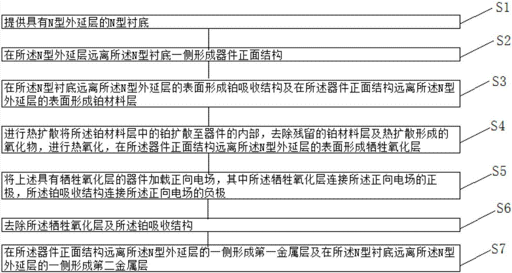
[0030] In order to solve the technical problem of increasing device voltage drop and reducing device performance due to unsatisfactory defect concentration distribution of the fast recovery diode formed by the existing method, the invention provides a method for manufacturing the fast recovery diode. see Figure 1-Figure 7 , the figure 1 It is a flowchart of the manufacturing method of the fast recovery diode of the present invention, Figure 2-Figure 7 yes figure 1 Schematic diagram of the structure of each step ...


PUM

PropertyMeasurementUnit
thicknessaaaaaaaaaa
strengthaaaaaaaaaa

Abstract

The invention provides a manufacturing method of a fast recovery diode. The manufacturing method of the fast recovery diode comprises following steps: providing an N-type substrate with an N-type epitaxial layer; forming a device front structure at one side, far from the N-type substrate, of the N-type epitaxial layer; forming a platinum absorption structure on the surface, far from the N-type epitaxial layer, of the N-type substrate and forming a platinum material layer on the surface, far from the N-type epitaxial layer, of the device front structure; performing thermal diffusion to diffuseplatinum in the platinum material layer to the internal part of a device; removing the remaining platinum material layer and an oxide formed by thermal diffusion, performing thermal oxidation, and forming a sacrifice oxide layer on the surface, far from the N-type epitaxial layer, of the device front structure; loading a forward electric field to the device with the sacrifice oxide layer, whereinthe sacrifice oxide layer is connected with a positive voltage of the forward electric field, and the platinum absorption structure is connected with a negative voltage of the forward electric field;and removing the sacrifice oxide layer and the platinum absorption structure.

Description

【Technical field】 [0001] The invention relates to the technical field of manufacturing semiconductor devices, in particular to a method for manufacturing a fast recovery diode. 【Background technique】 [0002] Whether the main circuit in the modern power electronic circuit is a thyristor with commutation shutdown or a new type of power electronic device with self-shutdown capability, such as GTO, MOSFET, IGBT, etc., it needs a power fast recovery diode connected in parallel. , to pass the reactive current in the load, reduce the charging time of the main switching device capacitor, and at the same time suppress the high voltage induced by the parasitic inductance when the load current reverses instantaneously. In recent years, with the continuous improvement of power semiconductor device manufacturing technology, the design and manufacture of new power semiconductor devices such as VDMOS and IGBT, the main switching devices in power electronic circuits, have made great progre...

Claims


Application Information

Patent Timeline
Patent Type & Authority Applications(China)
IPC IPC(8): H01L21/329
CPCH01L29/6603
Inventor 不公告发明人
Owner 山东鲁磁电子有限公司
Why Eureka
Try Eureka