

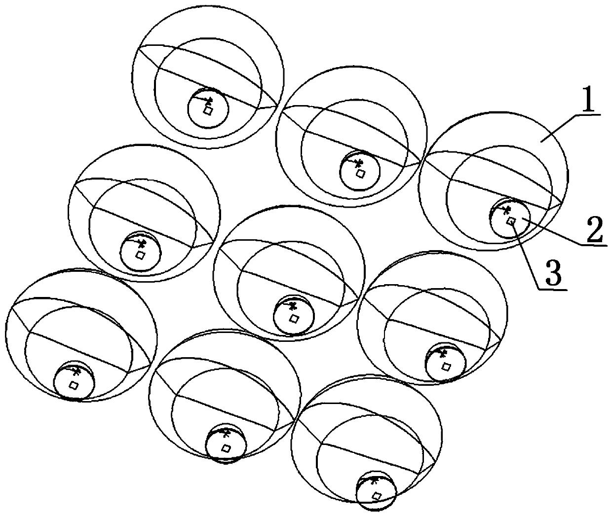
LED lens array design method for forming uniform square light spots
A technology of LED lens and square spot, which is applied in the direction of lens, semiconductor device of light-emitting element, optics, etc., can solve the problems of inability to control the small angle of LED light source, weak control of light source array uniformity, uneven illumination of the illuminated surface, etc., to achieve The boundary of the spot is clearly visible, the effect of spotlight is good, and the light is controllable
- Summary
- Abstract
- Description
- Claims
- Application Information
AI Technical Summary
Problems solved by technology
Method used
Image

Examples
Embodiment 1
[0047] The light source used in this embodiment is an LED light source with a size of 1mm*1mm; its specific design method is as follows:
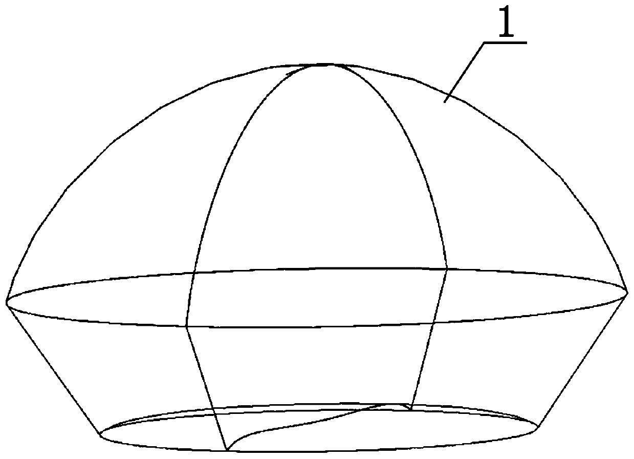
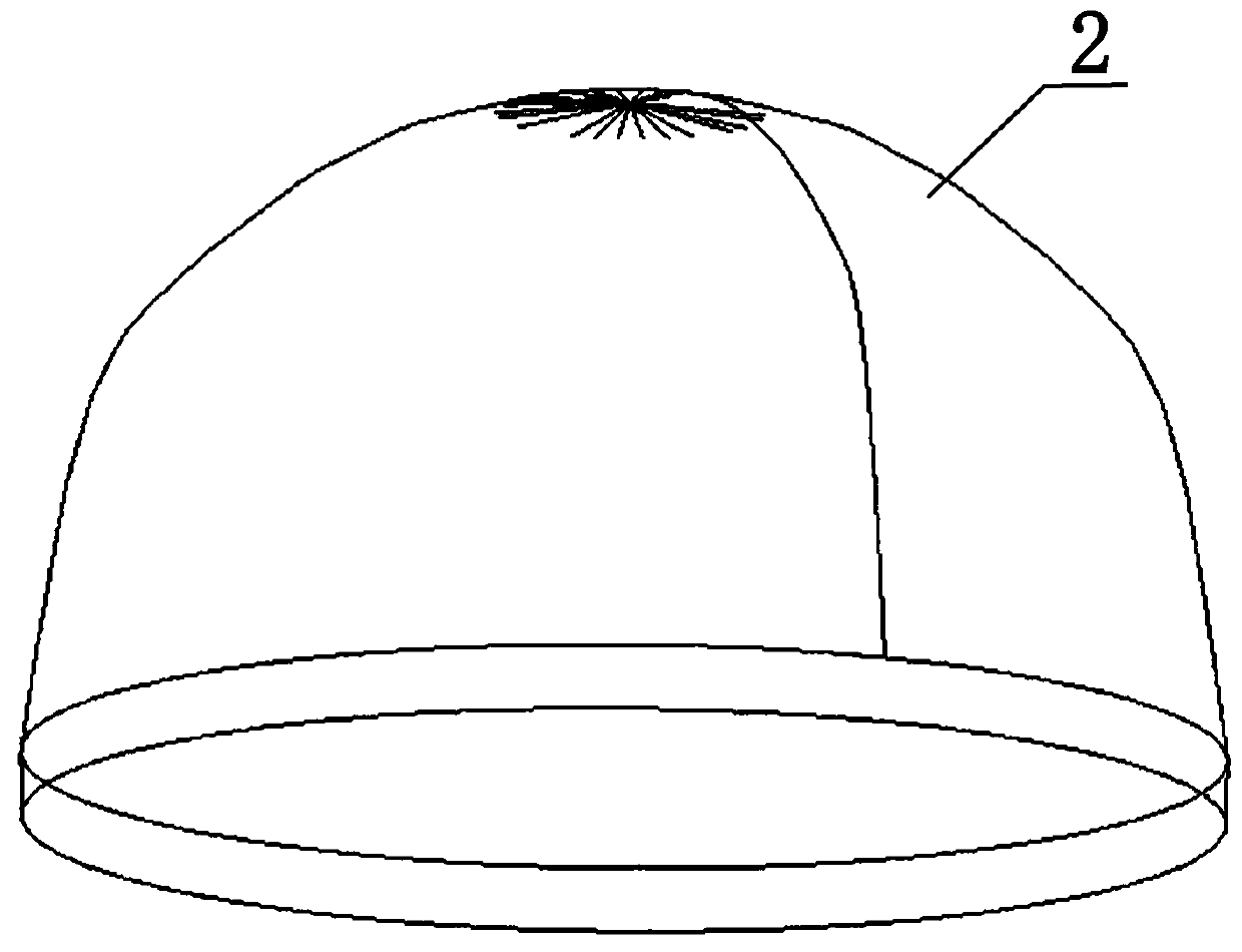
[0048] First, design the double free-form surface collimator lens, mainly including, 1) complete the derivation of the iterative relationship between the discrete point coordinates of the double free-form curve; 2) calculate the trajectory discrete coordinates of the free-form curve through Matlab computing software; 3) import the trajectory discrete coordinates into TracePro optics The simulation software establishes the solid lens model;
[0049] Among them, the iterative relationship of discrete points on double free curves is derived based on the theory of non-imaging optics, using the principle of energy conservation and Fresnel's law. In order to obtain the iterative relationship, a rectangular coordinate system is established, and any two adjacent two points are defined as A n 、A n+1 、B n 、B n+1 , whose coordinates are (xa n ,ya...
PUM
 Abstract
Description
Claims
Application Information