Microwave detection component and microwave detector
A technology of microwave detection and components, which is applied in the field of microwave detection, can solve problems such as limited use range, and achieve the effects of high signal-to-noise ratio, low power consumption, and high sensitivity
- Summary
- Abstract
- Description
- Claims
- Application Information
AI Technical Summary
Problems solved by technology
Method used
Image

Examples
Embodiment 1
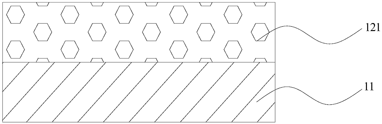
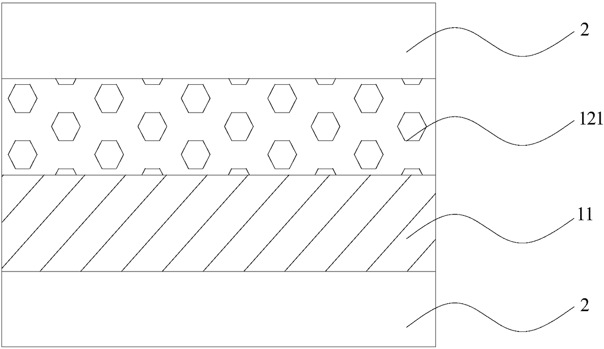
[0039] refer to figure 1 , this embodiment discloses a microwave detection element, which includes an insulating layer 11 and a first magnetic layer 121 arranged in layers; the insulating layer 11 and the first magnetic layer 121 are directly attached together; When a bias voltage is applied to the element, the insulating layer 11 will induce the bias voltage, and the interface of the insulating layer 11 adjacent to the first magnetic layer 121 will undergo stress deformation and act on the first magnetic layer 121. The first magnetic layer 121 The magnetic properties of the ions are changed, that is, the first magnetic layer 121 is modulated by the electric field for microwave detection.
[0040] In the microwave detection element of this embodiment, the above-mentioned electric field regulation mechanism is called stress regulation.
[0041] In the present embodiment, since the microwave detection element is a double-layer structure with only one magnetic layer, its magneto...
Embodiment 2
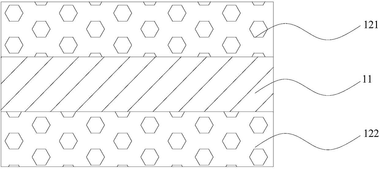
[0048] refer to image 3 As shown, Embodiment 2 discloses a microwave detection element, which includes a first magnetic layer 121 , an insulating layer 11 and a second magnetic layer 122 which are arranged in layers.
[0049] It should be noted that, in the microwave detection element of this embodiment, the mechanism of electric field regulation is specifically interface regulation. Specifically, the bias voltage is applied through two pieces of metal electrodes (not shown in the figure) attached to the two sides of the first magnetic layer 121 and the second magnetic layer 122 respectively; when the bias voltage is applied to the microwave detection element , the insulating layer 11 generates an electric field, and this part of the electric field only acts on a few atomic layer thick regions of the interface between the first magnetic layer 121 and the insulating layer 11 due to the shielding effect of free electrons, and affects the first magnetic layer 121. Magnetic prop...
Embodiment 3
[0061] In the description of Embodiment 3, the similarities with Embodiment 2 will not be repeated here, and only the differences with Embodiment 2 will be described. Specific reference Image 6 As shown, the difference between Embodiment 3 and Embodiment 2 is that the thickness of the insulating layer 11 is 0.5 nm to 5 nm, and the material of the insulating layer 11 is selected from Al 2 O 3 and at least one of MgO; the thickness of the first magnetic layer 121 does not exceed 2 nm.
[0062] In this embodiment, a non-magnetic metal layer 13 is also preferably disposed on the insulating layer 11; that is, the microwave detection element disclosed in this embodiment includes a first magnetic layer 121, an insulating layer 11 and a non-magnetic layer 121, which are stacked in sequence. Magnetic metal layer 13 .
[0063] Specifically, the thickness of the non-magnetic metal layer 13 is 5 nm, and the material of the non-magnetic metal layer 13 is selected from at least one of C...
PUM
 Abstract
Description
Claims
Application Information
 - R&D
- Intellectual Property
- Life Sciences
- Materials
- Tech Scout
- Unparalleled Data Quality
- Higher Quality Content
- 60% Fewer Hallucinations
Browse by: Latest US Patents, China's latest patents, Technical Efficacy Thesaurus, Application Domain, Technology Topic, Popular Technical Reports.
© 2025 PatSnap. All rights reserved.Legal|Privacy policy|Modern Slavery Act Transparency Statement|Sitemap|About US| Contact US: help@patsnap.com