OLED panel, manufacturing method therefor, and display device

A manufacturing method and panel technology, applied in semiconductor/solid-state device manufacturing, semiconductor devices, electrical components, etc., can solve problems such as complex process, low display brightness, large square resistance of transparent cathode, etc., to simplify process conditions and simplify manufacturing process , the effect of reducing the production cost

Active Publication Date: 2018-05-25
HEFEI XINSHENG OPTOELECTRONICS TECH CO LTD +1
View PDF5 Cites 11 Cited by
  • Summary
  • Abstract
  • Description
  • Claims
  • Application Information

AI Technical Summary

Problems solved by technology

[0004] In order to increase the light transmittance, the cathode needs to use a thinner transparent conductive material, but the thinner transparent cathode has a large square resistance, and a large voltage drop will occur when the current flows through the cathode. Therefore, the farther the distance from the power supply point is The smaller the cathode voltage obtained on the distant pixel, the lower the display brightness of the pixel compared with the display brightness of the pixel closer to the power supply point, which makes the brightness uniformity of the OLED display device worse
[0005] In order to solve this problem, the prior art proposes to set an auxiliary electrode with a small resistance on the color filter substrate to reduce the resistance of the cathode, but the process is complicated and it is easy to cause an open circuit between the cathode and the auxiliary electrode.

Method used


Image

  • OLED panel, manufacturing method therefor, and display device
  • OLED panel, manufacturing method therefor, and display device
  • OLED panel, manufacturing method therefor, and display device

Examples


Embodiment Construction

[0031] The present invention will be further described below with reference to the accompanying drawings and exemplary embodiments, wherein the same reference numerals in the accompanying drawings all refer to the same components. Also, detailed descriptions of known arts will be omitted if they are unnecessary to illustrate the features of the present invention.

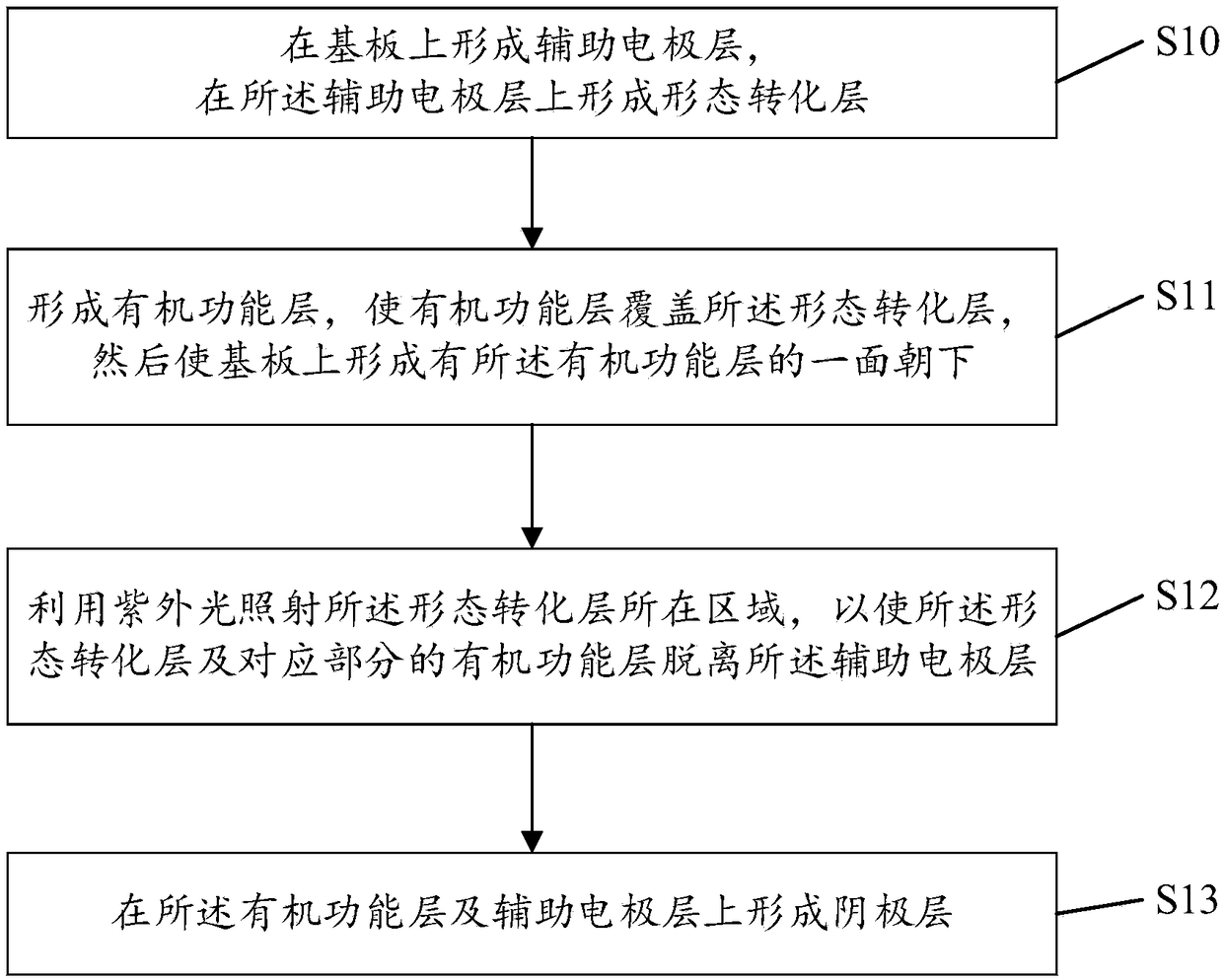
[0032] The present invention provides a method for manufacturing an OLED panel, the flow diagram of which is shown in Figure 1, and the specific steps are as follows:

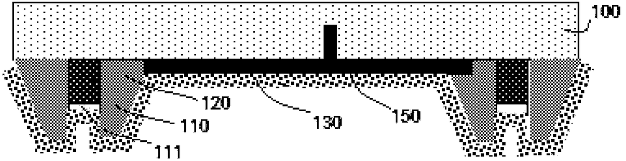
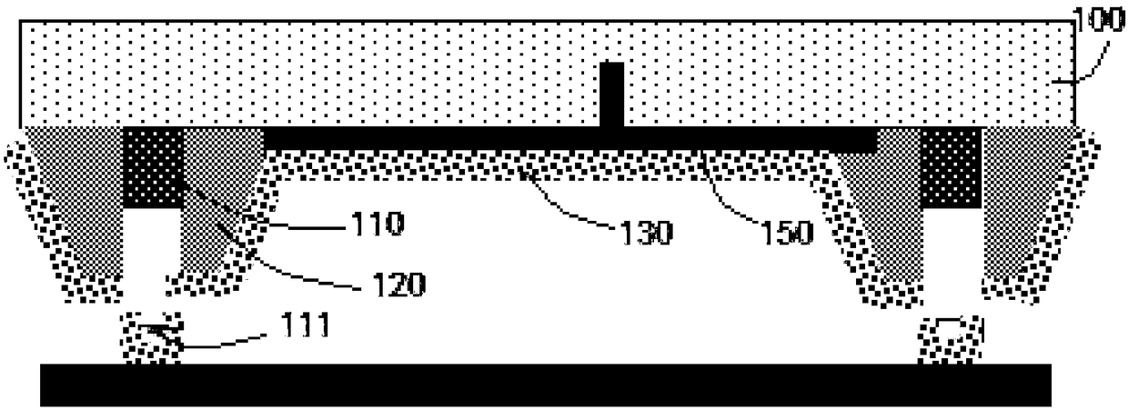
[0033] S10, forming an auxiliary electrode layer on the substrate, and forming a morphology conversion layer on the auxiliary electrode layer;

[0034] Specifically, the auxiliary electrode layer can be deposited by evaporation, sputtering, or inkjet printing, and the morphology conversion layer can be fixed on the auxiliary electrode layer by inkjet printing, evaporation, etc., so that the morphology conversion layer covers the auxiliary electrode l...


PUM

PropertyMeasurementUnit
thicknessaaaaaaaaaa
electrical resistivityaaaaaaaaaa
thicknessaaaaaaaaaa

Abstract

The invention relates to the technical field of display, and especially relates to an OLED panel, a manufacturing method therefor, and a display device. The manufacturing method for the OLED panel comprises the steps: forming an auxiliary electrode layer on a substrate, and forming a form transformation layer on the auxiliary electrode layer; forming an organic function layer, enabling the organicfunction layer to cover the form transformation layer, and then enabling one surface of the organic function layer formed on the substrate to face downwards; irradiating a region where the form transformation layer is located through ultraviolet light so as to enable the form transformation layer and a corresponding part of the organic function layer to break away from the auxiliary electrode layer; and forming cathode layers on the organic function layer and the auxiliary electrode layer. According to the technical scheme of the invention, the method can achieve the effective connection of the auxiliary electrode layer and the cathode layers, thereby reducing the voltage drop of the cathode layers, improving the uniformity of brightness display, and simplifying the manufacturing technology of the OLED panel.

Description

【Technical field】 [0001] The invention relates to the field of display technology, in particular to an OLED panel, a manufacturing method thereof, and a display device. 【Background technique】 [0002] In recent years, OLED (Organic Light-Emitting Diode, Organic Light-Emitting Diode) has become the most promising new display device in recent years due to its advantages of self-luminescence, all-solid-state, high contrast, etc. [0003] A pixel structure includes an array substrate and a color filter substrate, and the array substrate includes a thin film transistor device layer, an anode layer, a light emitting layer and a cathode layer formed on the first substrate. When the display panel is working, a voltage is applied between the anode and the cathode, so that the light-emitting layer is excited to emit light, and the light passes through the transparent cathode and the color filter substrate on the top to achieve top emission. [0004] In order to increase the light tra...

Claims


Application Information

Patent Timeline
Patent Type & Authority Applications(China)
IPC IPC(8): H01L51/52H01L51/56H01L27/32
CPCH10K59/12H10K50/85H10K50/86H10K71/00H10K59/1315H10K59/1795H10K71/221H10K50/818H10K50/824H10K59/122H10K59/131H10K71/191H10K50/11
Inventor 王欣欣贾文斌胡月宋丽芳叶志杰
Owner HEFEI XINSHENG OPTOELECTRONICS TECH CO LTD
Why Eureka
Try Eureka