Composite material for filling vertical through silicon via (TSV) and filling method thereof

A technology of composite materials and filling methods, which is used in the manufacture of electrical components, circuits, semiconductor/solid-state devices, etc., to achieve the effect of improving reliability

Inactive Publication Date: 2018-06-01
HUAZHONG UNIV OF SCI & TECH
View PDF3 Cites 7 Cited by
  • Summary
  • Abstract
  • Description
  • Claims
  • Application Information

AI Technical Summary

Problems solved by technology

However, due to the small pore size of TSV, it is difficult to fill TSV with composite materials, so Cu and other materials are usually used for filling. There

Method used


Image

  • Composite material for filling vertical through silicon via (TSV) and filling method thereof
  • Composite material for filling vertical through silicon via (TSV) and filling method thereof
  • Composite material for filling vertical through silicon via (TSV) and filling method thereof

Examples


Embodiment 1

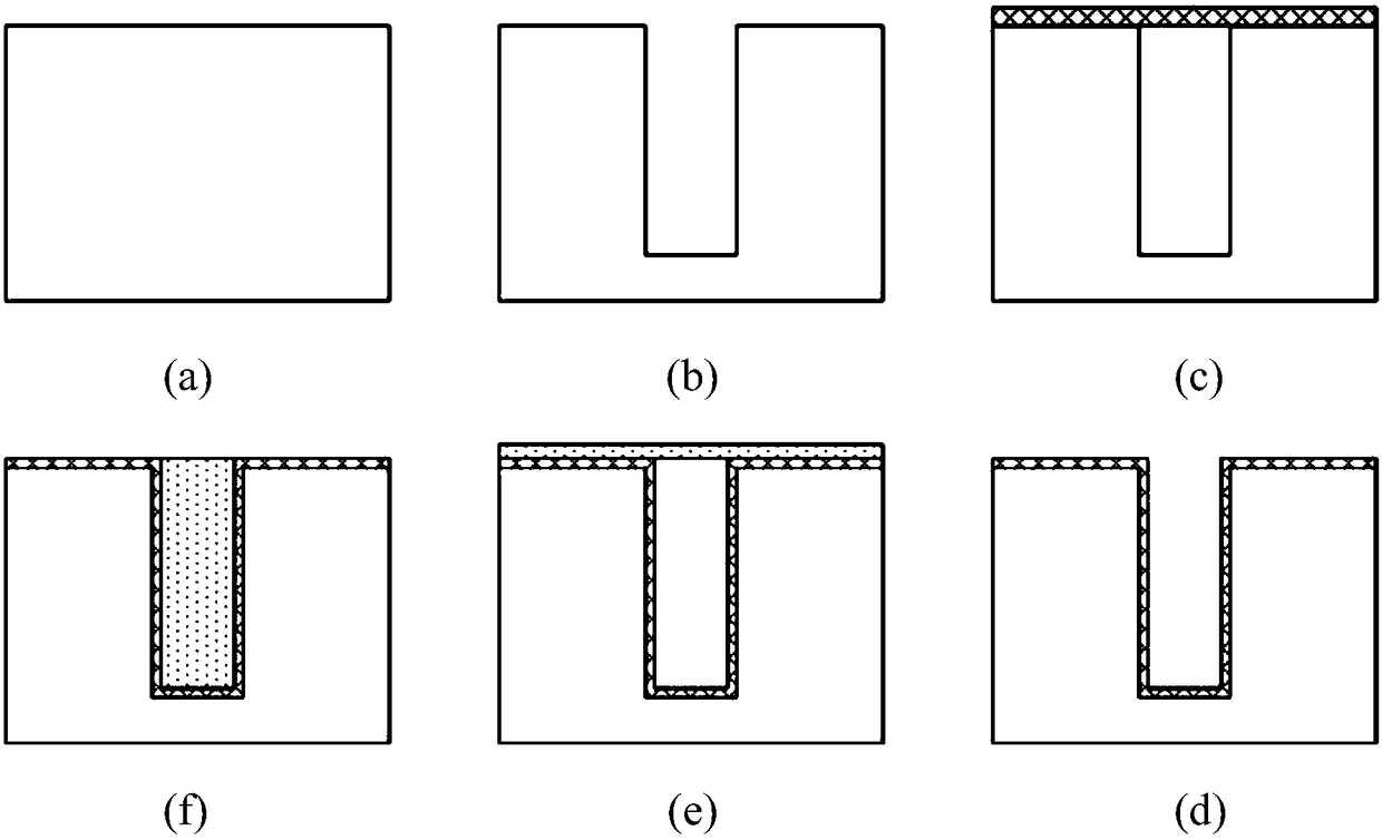
[0052] Step 1: Use deep reactive ion etching (DRIE) or inductively coupled plasma technology (ICP) to etch a through hole on the silicon wafer. The thickness of the silicon wafer is 50um ~ 300um. The hole can be a round hole or a square hole. Pores with a diameter of 0um to 200um and an aspect ratio of 5:1 to 20:1;

[0053] Step 2: Rinse with deionized water to eliminate residual ions on the surface of the wafer and blind holes, and dry in a drying oven under a protective atmosphere;

[0054] Step 3: On the surface of the through hole, an adhesion layer, a barrier layer and a seed layer are sequentially layered. The thickness of the adhesion layer is about 50nm~100nm, the thickness of the barrier layer is about 0.5um~1um, and the thickness of the seed layer is 0.5um~ 1um; the material of the adhesion layer is selected TiN, grown by sputtering method, the material of the barrier layer is selected as SiO2, deposited by vacuum vapor deposition technology, the material of the meta...

Embodiment 2

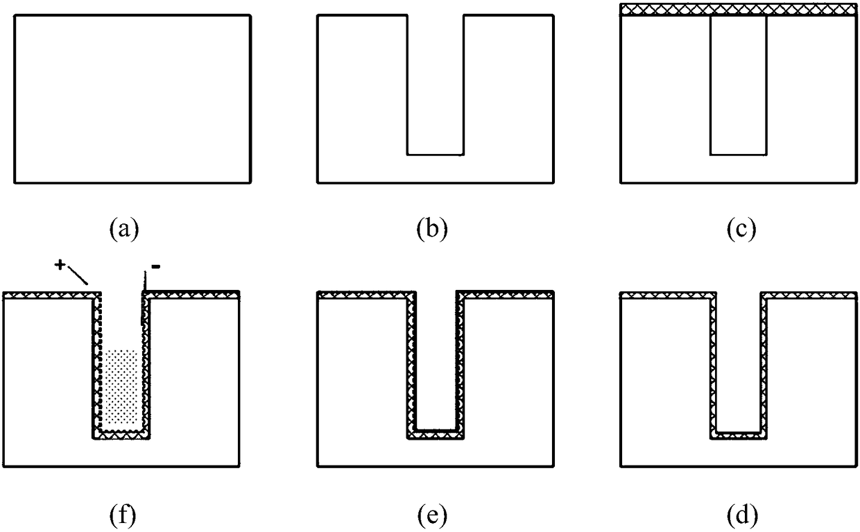
[0076] Step 1: Use deep reactive ion etching (DRIE) or inductively coupled plasma technology (ICP) to etch a through hole on the silicon wafer. The thickness of the silicon wafer is 50um ~ 300um. The hole can be a round hole or a square hole. Pores with a diameter of 0um to 200um and an aspect ratio of 5:1 to 20:1;

[0077] Step 2: Rinse with deionized water to eliminate residual ions on the surface of the wafer and blind holes, and dry in a drying oven under a protective atmosphere;

[0078] Step 3: On the surface of the through hole, an adhesion layer, a barrier layer and a seed layer are sequentially layered. The thickness of the adhesion layer is about 50nm~100nm, the thickness of the barrier layer is about 0.5um~1um, and the thickness of the seed layer is 0.5um~ 1um; the material of the adhesion layer is selected TiN, grown by sputtering method, the material of the barrier layer is selected as SiO2, deposited by vacuum vapor deposition technology, the material of the meta...

Embodiment 3

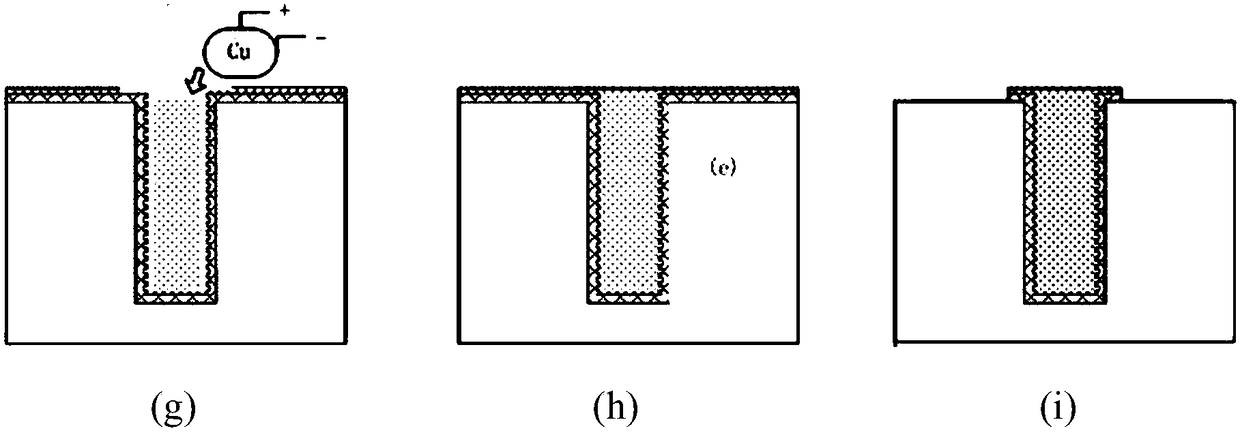
[0100] Step 1: Use deep reactive ion etching (DRIE) or inductively coupled plasma technology (ICP) to etch a through hole on the silicon wafer. The thickness of the silicon wafer is 50um-300um. The pore size is larger than the lower pore size, but not more than 1 / 2. Usually the upper pore size is 50-200um, the lower pore size is 0-150um, and the through-hole aspect ratio is 5:1-20:1;

[0101] Step 2: Rinse with deionized water to eliminate residual ions on the surface of the wafer and blind holes, and dry in a drying oven under a protective atmosphere;

[0102] Step 3: On the surface of the through hole, an adhesion layer, a barrier layer and a seed layer are sequentially layered. The thickness of the adhesion layer is about 50nm~100nm, the thickness of the barrier layer is about 0.5um~1um, and the thickness of the seed layer is 0.5um~ 1um; the material of the adhesion layer is selected TiN, grown by sputtering method, the material of the barrier layer is selected as SiO2, dep...


PUM

PropertyMeasurementUnit
Diameteraaaaaaaaaa
Thermal expansion coefficientaaaaaaaaaa
Thermal conductivityaaaaaaaaaa

Abstract

The invention discloses a composite material for filling a vertical through silicon via (TSV) and a filling method thereof, wherein the composite material is mainly composed of diamond and copper, thediameter of the diamond is less than 1 [mu]m, and the diamond is monocrystal diamond or boron-doped diamond. The filling method comprises sputtering an adhesion layer, a barrier layer, and a seed layer in the TSV in advance, depositing the composite material by a composite electrodeposition method, and then attaching and depositing the copper atoms along a current direction to fully fill the TSVby energization so as to form a completely filled composite layer on a silicon wafer. By the key internal composition and structure of the composite material, the overall process flow design of the corresponding filling method, and the improvements in conditions and parameters of each step, and using a specific composite material as a TSV filling material and using a specific filling method, the reliability of the TSV can be improved and the failure rate of the TSV can be reduced to avoid filling defects.

Description

technical field [0001] The invention belongs to the technical field of microelectronics manufacturing or processing semiconductor or solid device methods, and more particularly relates to a composite material for filling vertical TSVs and a filling method thereof, which can effectively improve the reliability of TSV devices. Background technique [0002] The integration of integrated circuits is constantly improving, and semiconductor technology continues to develop rapidly. At present, the improvement of integration is mainly to reduce the minimum feature size. The minimum feature size is gradually reduced from 90 nanometers to 14 nanometers, and the breakthrough to the so-called physical limit of 10 nanometers enables the integration of more components in a given area. . However, the above-mentioned reduction of the minimum feature size is basically two-dimensional integration, that is, integrating as many components as possible on the semiconductor wafer plane, but as in...

Claims


Application Information

Patent Timeline
IPC IPC(8): H01L21/768
CPCH01L21/76879
Inventor 程晓敏陈高翔宋夷斌缪向水
Owner HUAZHONG UNIV OF SCI & TECH
Why Eureka
Try Eureka