Light emitting diode and preparation method thereof

A technology of light-emitting diodes and substrates, which is applied in the direction of electrical components, circuits, semiconductor devices, etc., can solve the problems of internal quantum efficiency improvement, high electron barrier layer, and difficult preparation, so as to reduce the difficulty of preparation, reduce the aluminum component, Effect of increasing electron-hole wavefunction overlap

Active Publication Date: 2018-06-01
XIAMEN CHANGELIGHT CO LTD
View PDF4 Cites 6 Cited by
  • Summary
  • Abstract
  • Description
  • Claims
  • Application Information

AI Technical Summary

Problems solved by technology

In addition, ultraviolet light-emitting diodes are used in many fields, such as ultraviolet curing, air and water purification, daily lighting, etc. However, due to the limitation of production technology level at this stage, there are still many problems in the large-scale application of ultraviolet light-emitting diodes. The structure of the light-emitting diode in the ultraviolet band in the technology mainly includes a substrate, a buffer layer, an aluminum gallium nitrogen current spreading layer, a multi-quantum well layer, an electron blocking layer and a P-type contact layer, because the average aluminum composition of the electron blocking layer is relatively high , it is difficult to prepare, and due to the strong polarization field between the electron blocking layer and the last quantum barrier in the multi-quantum well layer, it is not conducive to the radiative recombination of electron holes, which limits the further improvement of the internal quantum efficiency of light-emitting diodes. promote

Method used


Image

  • Light emitting diode and preparation method thereof
  • Light emitting diode and preparation method thereof
  • Light emitting diode and preparation method thereof

Examples


Embodiment Construction

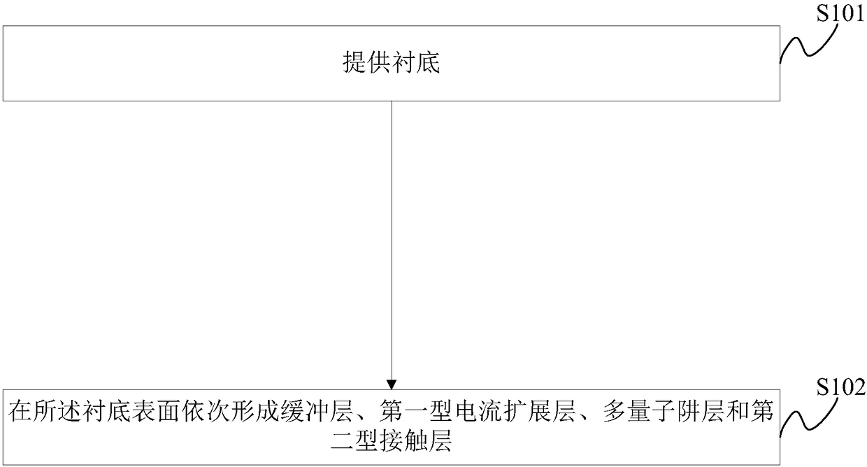
[0047] The following will clearly and completely describe the technical solutions in the embodiments of the application with reference to the drawings in the embodiments of the application. Apparently, the described embodiments are only some of the embodiments of the application, not all of them. Based on the embodiments in this application, all other embodiments obtained by persons of ordinary skill in the art without making creative efforts belong to the scope of protection of this application.

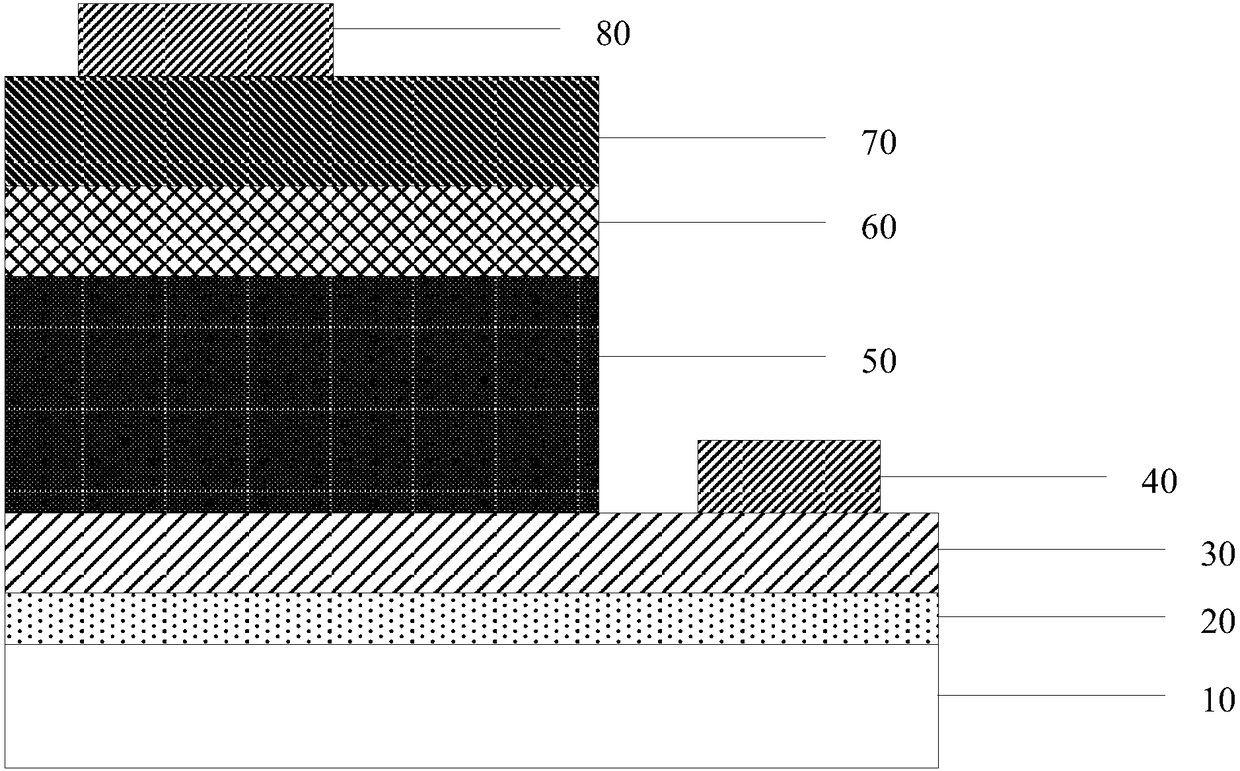
[0048] The embodiment of the present application provides a light emitting diode, such as figure 1 shown, including:

[0049] Substrate;

[0050] A buffer layer, a first-type current spreading layer, a multi-quantum well layer and a second-type contact layer stacked in sequence on the surface of the substrate; wherein,

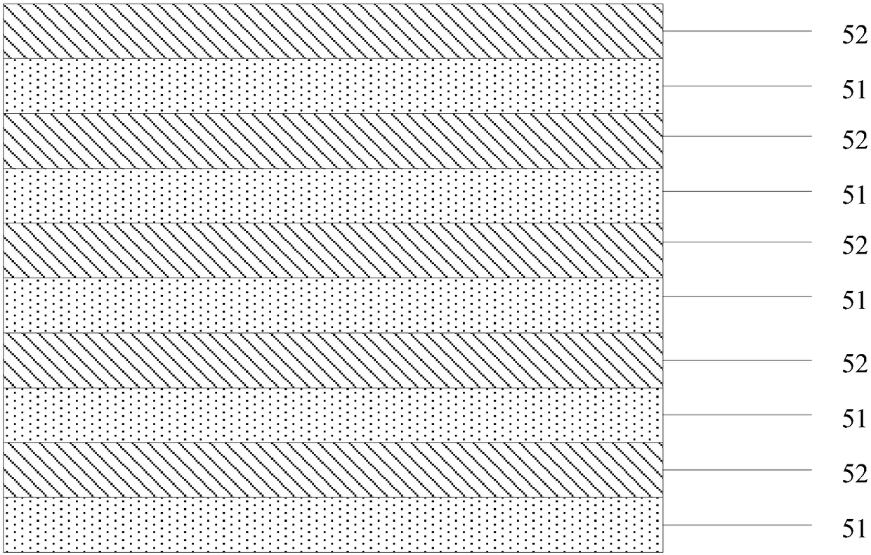
[0051] The multi-quantum well layer includes a plurality of stacked quantum periodic layers and a superlattice structure located on the side away from the substra...


PUM


Abstract

The application discloses a light emitting diode and a preparation method thereof. According to the light emitting diode, the last quantum barrier layer of a plurality of quantum well layers and an electron blocking layer in a conventional structure are replaced with a super lattice structure comprising a plurality of first-type super lattice layers and a plurality of second-type super lattice layers; the super lattice structure reduces polarization electric field intensity of the last quantum barrier layer, improves an electron hole wave function overlapping degree of the light emitting diodeand is beneficial to radiation composite light emitting of the light emitting diode; and the super lattice structure not only reduces the preparation difficulty of the light emitting diode, but alsoenables growth of the high-quality super lattice structure and second-type contact layer to be possible. In addition, existence of the super lattice structure also enables a electronic barrier heightof a conduction band of the integral second-type structural layer to be further increased, greatly reduces electron leakage, meanwhile, reduces a barrier height of a valence band hole, promotes transmission of the hole, greatly promotes internal quantum efficiency of multiple quantum well layers, reduces sudden reduction of efficiency, and greatly promotes integral light emitting power of the light emitting diode.

Description

technical field [0001] The present application relates to the technical field of semiconductors, and more specifically, to a light emitting diode and a preparation method thereof. Background technique [0002] A light emitting diode (Light Emitting Diode, LED), also called an electroluminescent diode, is a core component of an LED lamp. With the rapid development of light-emitting diode technology, light-emitting diodes are more and more widely used in various fields. [0003] III-V nitrides, due to their direct bandgap semiconductor characteristics, have excellent physical properties such as large forbidden band width, high breakdown electric field, and high electron saturation mobility, and have received extensive attention in the fields of electronics and optics. Among them, blue and white light-emitting diodes based on GaN as the main material have achieved higher efficiency than any conventional light source, and are widely used in various emerging industries. However...

Claims


Application Information

Patent Timeline
Patent Type & Authority Applications(China)
IPC IPC(8): H01L33/06
CPCH01L33/06
Inventor 万志卓祥景孙传平林志伟尧刚
Owner XIAMEN CHANGELIGHT CO LTD
Why Eureka
Try Eureka