Preparation method of absorption layer of copper-indium-gallium-selenium solar battery

A technology for solar cells and copper indium gallium selenide, which is applied in the field of solar cells, can solve the problems of difficulty in controlling the processing quality of the film layer, complicated preparation process of the CIGS absorption layer, etc., so as to improve the production efficiency, solve the problems of low control precision and simplify the processing technology. Effect

Inactive Publication Date: 2018-06-05
BEIJING APOLLO DING RONG SOLAR TECH
View PDF10 Cites 2 Cited by
  • Summary
  • Abstract
  • Description
  • Claims
  • Application Information

AI Technical Summary

Problems solved by technology

[0003] However, the disadvantage of the prior art is that the preparation process of the CIGS absorbing layer is complicated, and it needs to be selenized after multi-step sputtering
Since the sputtering of each layer requires precise control and adjustment of the optimal element content ratio to meet the requirements of CIGS preparation, it is difficult to control the processing quality of each film layer

Method used


Image

  • Preparation method of absorption layer of copper-indium-gallium-selenium solar battery
  • Preparation method of absorption layer of copper-indium-gallium-selenium solar battery

Examples


Embodiment Construction

[0028] Embodiments of the present invention are described in detail below, examples of which are shown in the drawings, wherein the same or similar reference numerals designate the same or similar elements or elements having the same or similar functions throughout. The embodiments described below by referring to the figures are exemplary only for explaining the present invention and should not be construed as limiting the present invention.

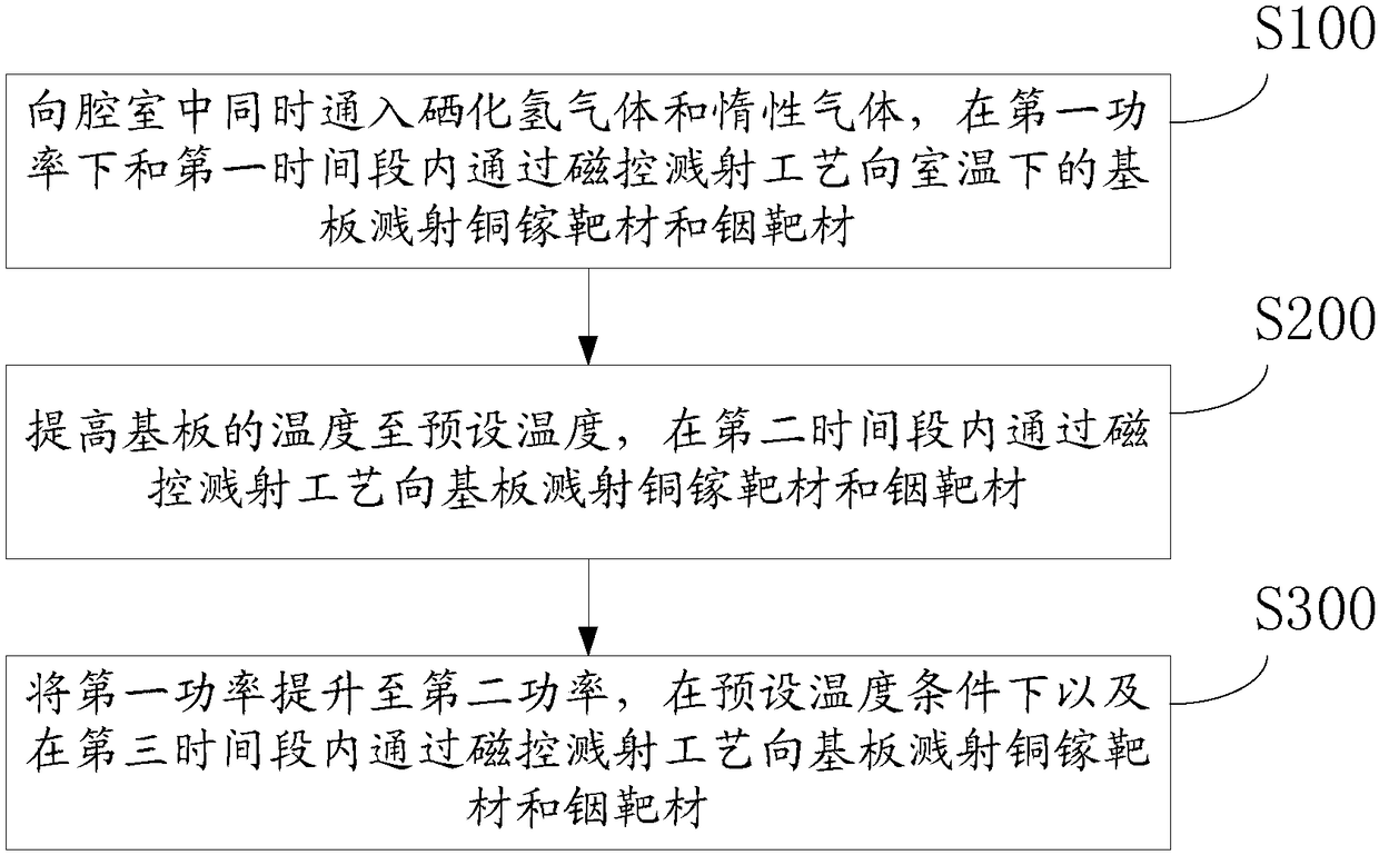
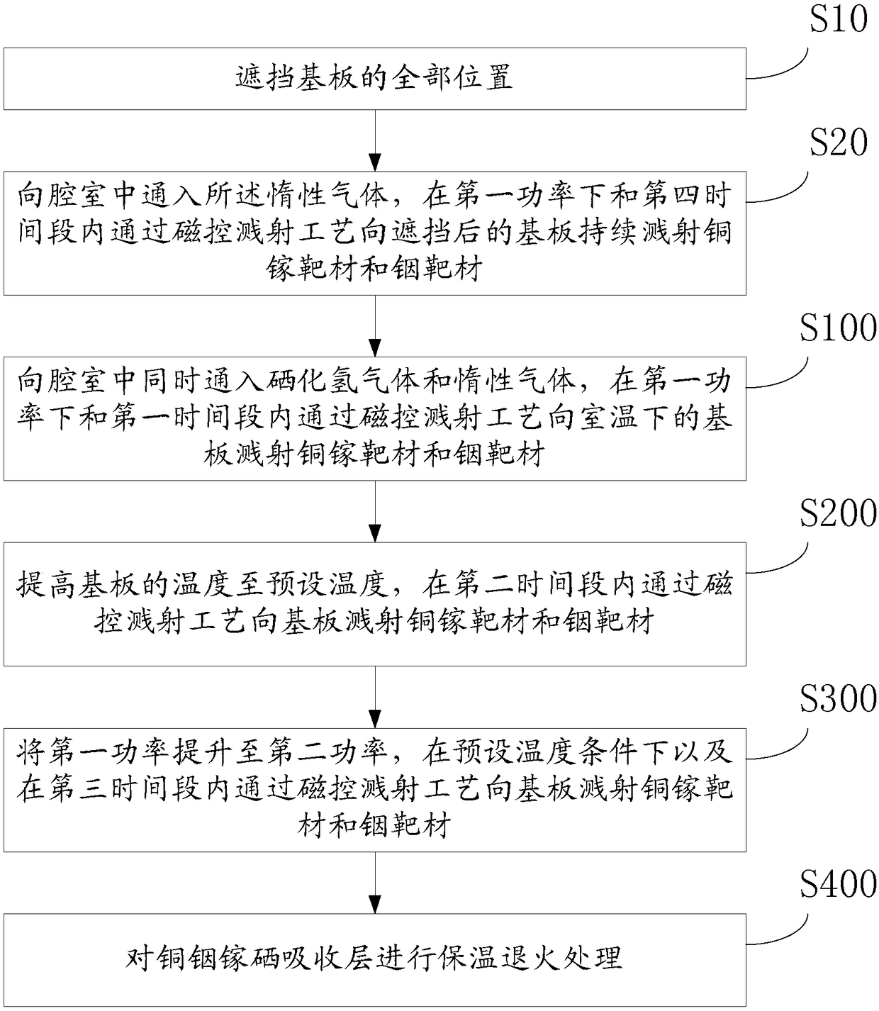
[0029] Such as figure 1 As shown, the embodiment of the present invention provides a method for preparing an absorber layer of a copper indium gallium selenide (CIGS) solar cell, which includes the following steps:

[0030] S100. Simultaneously feed hydrogen selenide (H2Se) gas and inert gas into the chamber, and sputter a copper gallium (CuGa) target to the substrate at room temperature through a magnetron sputtering process under the first power and within the first time period. material and indium (In) target.

[0031] S200. Increas...


PUM


Abstract

The invention discloses a preparation method of an absorption layer of a copper-indium-gallium-selenium solar battery. The preparation method comprises the following steps: simultaneously inflating hydrogen selenide gas and inert gas into a chamber, sputtering a copper-gallium target material and an indium target material onto a substrate at room temperature by a magnetron sputtering technology under first power and within a first time period; raising the temperature of the substrate to a preset temperature, and sputtering the copper-gallium target material and the indium target material ontothe substrate by the magnetron sputtering technology within a second time period; increasing the first power to second power, and sputtering the copper-gallium target material and the indium target material onto the substrate by the magnetron sputtering technology under a preset temperature condition and within a third time period. By the preparation method of the absorption layer of the copper-indium-gallium-selenium solar battery, provided by the invention, through simultaneous sputtering of the CuGa target material and the In target material in an H2Se atmosphere, the CIGS absorption layercan be moulded in a sputtering manner in only one step, so that the processing technology is effectively simplified, and the production efficiency and the control precision are improved.

Description

technical field [0001] The invention relates to the technical field of solar cells, in particular to a method for preparing an absorbing layer of a copper indium gallium selenide solar cell. Background technique [0002] Cu(In,Ga)Se2(CIGS) is a direct bandgap semiconductor. With the doping of Ga element, the bandgap width of CIGS can be adjusted between 1.02eV and 1.68eV. CIGS has a high absorption coefficient for visible light and is the most promising material for making high-efficiency and low-cost thin-film solar cells. The current magnetron sputtering technology to prepare the CIGS battery absorber layer is to prepare the CIGS precursor film by sputtering multiple targets (such as single target sputtering, copper-rich target and copper-poor target at the same time or successively sputtering), and then the CIGS precursor film Heat treatment: heating the elemental Se source in a vacuum or an inert atmosphere with a certain pressure to form a saturated vapor pressure of S...

Claims


Application Information

Patent Timeline
Patent Type & Authority Applications(China)
IPC IPC(8): H01L31/032H01L31/0749C23C14/35C23C14/06
CPCC23C14/0057C23C14/0623C23C14/35H01L31/0322H01L31/0749Y02E10/541Y02P70/50
Inventor 聂曼
Owner BEIJING APOLLO DING RONG SOLAR TECH
Why Eureka
Try Eureka