Preparation method of metal nano-network flexible panel for electronic information display
A metal nano network, flexible panel technology, applied in metal/alloy conductors, cable/conductor manufacturing, circuits, etc., can solve the problems of high production cost, unmaintainable, complex process, etc.
- Summary
- Abstract
- Description
- Claims
- Application Information
AI Technical Summary
Problems solved by technology
Method used
Image
Examples
Embodiment 1
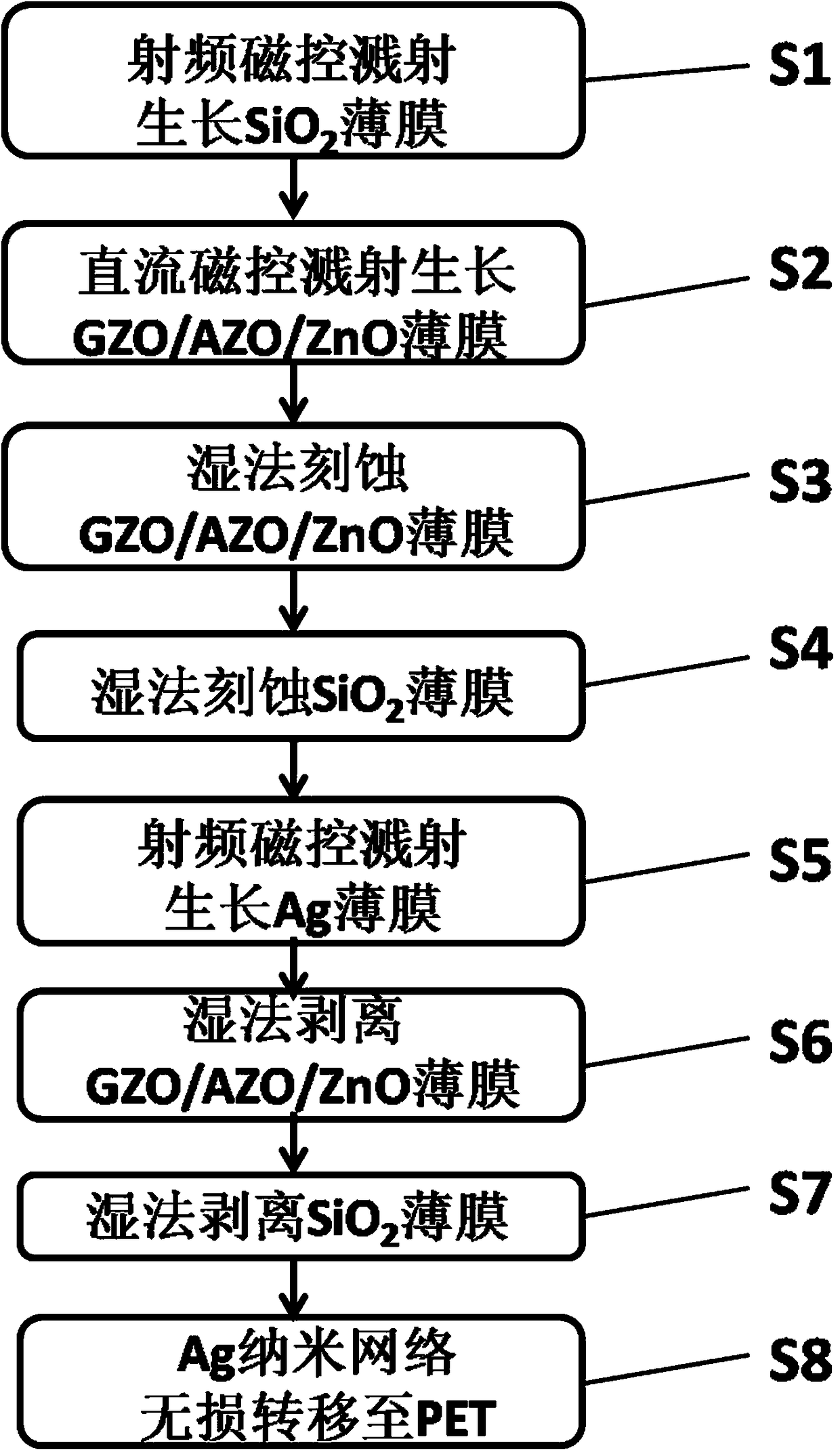
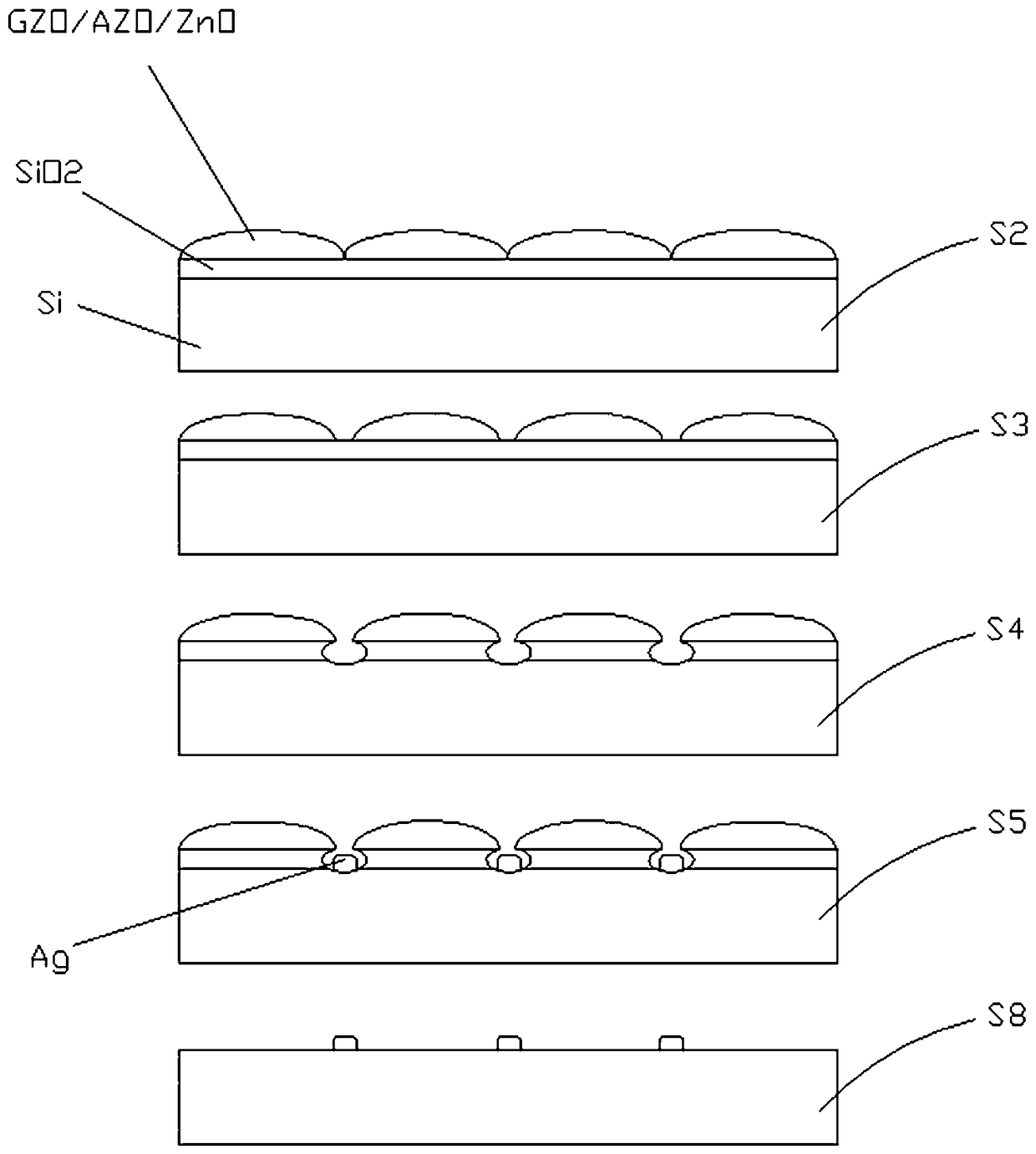
[0029] Such as figure 1 and figure 2 As shown, a method for preparing a metal nano-network flexible panel for electronic information display provided by the present invention comprises the following steps:
[0030] S1, using silicon ceramics as the substrate, placing the substrate in the magnetron sputtering chamber, using Ar ions as the sputtering gas, O 2 As a reaction gas, the radio frequency power supply acts on the cathode, and the preparation temperature is kept at room temperature; the sputtering power is 250W, the working pressure is 0.5Pa, the target voltage is 87V, and the distance between the substrate and the target is 70mm, and the prepared SiO 2 A sacrificial layer with a film thickness of 300nm.
[0031] S2, using magnetron sputtering method, on SiO 2 GZO film was prepared on the film as a cover layer, GZO ceramic target was used, Ar ions were used as sputtering gas, DC power was applied to the cathode, sputtering power was 300W, working pressure was 0.2Pa, ...
Embodiment 2
[0040]A method for preparing a metal nano-network flexible panel for electronic information display provided by the present invention comprises the following steps:
[0041] S1, using silicon ceramics as the substrate, placing the substrate in the magnetron sputtering chamber, using Ar ions as the sputtering gas, O 2 As a reaction gas, the radio frequency power supply acts on the cathode, and the preparation temperature is kept at room temperature; the sputtering power is 250W, the working pressure is 0.5Pa, the target voltage is 87V, and the distance between the substrate and the target is 70mm, and the prepared SiO 2 A sacrificial layer with a film thickness of 300nm.
[0042] S2, using magnetron sputtering method, on SiO 2 The AZO film was prepared on the film as a cover layer, using AZO ceramic target material, Ar ions as sputtering gas, DC power supply on the cathode, sputtering power of 350W, working pressure of 0.2Pa, target voltage of 441V, flexible panel substrate an...
Embodiment 3
[0051] A method for preparing a metal nano-network flexible panel for electronic information display provided by the present invention comprises the following steps:
[0052] S1, using silicon ceramics as the substrate, placing the substrate in the magnetron sputtering chamber, using Ar ions as the sputtering gas, O 2 As a reaction gas, the radio frequency power supply acts on the cathode, and the preparation temperature is kept at room temperature; the sputtering power is 250W, the working pressure is 0.5Pa, the target voltage is 87V, and the distance between the substrate and the target is 70mm, and the prepared SiO 2 A sacrificial layer with a film thickness of 300nm.
[0053] S2, using magnetron sputtering method, on SiO 2 The ZnO thin film was prepared on the thin film as the covering layer, ZnO ceramic target was used, Ar ions were used as the sputtering gas, DC power was applied to the cathode, the sputtering power was 400W, the working pressure was 0.2Pa, the target v...
PUM
| Property | Measurement | Unit |
|---|---|---|
| thickness | aaaaa | aaaaa |
| thickness | aaaaa | aaaaa |
| electrical resistivity | aaaaa | aaaaa |
Abstract
Description
Claims
Application Information
 - R&D
- Intellectual Property
- Life Sciences
- Materials
- Tech Scout
- Unparalleled Data Quality
- Higher Quality Content
- 60% Fewer Hallucinations
Browse by: Latest US Patents, China's latest patents, Technical Efficacy Thesaurus, Application Domain, Technology Topic, Popular Technical Reports.
© 2025 PatSnap. All rights reserved.Legal|Privacy policy|Modern Slavery Act Transparency Statement|Sitemap|About US| Contact US: help@patsnap.com


