A method for preparing a metal nano-network flexible panel for electronic information display
A metal nano-network and flexible panel technology, which is applied in cable/conductor manufacturing, metal/alloy conductors, circuits, etc., can solve problems such as complex process, silver nanowire agglomeration, and increased contact resistance
- Summary
- Abstract
- Description
- Claims
- Application Information
AI Technical Summary
Problems solved by technology
Method used
Image
Examples
Embodiment 1
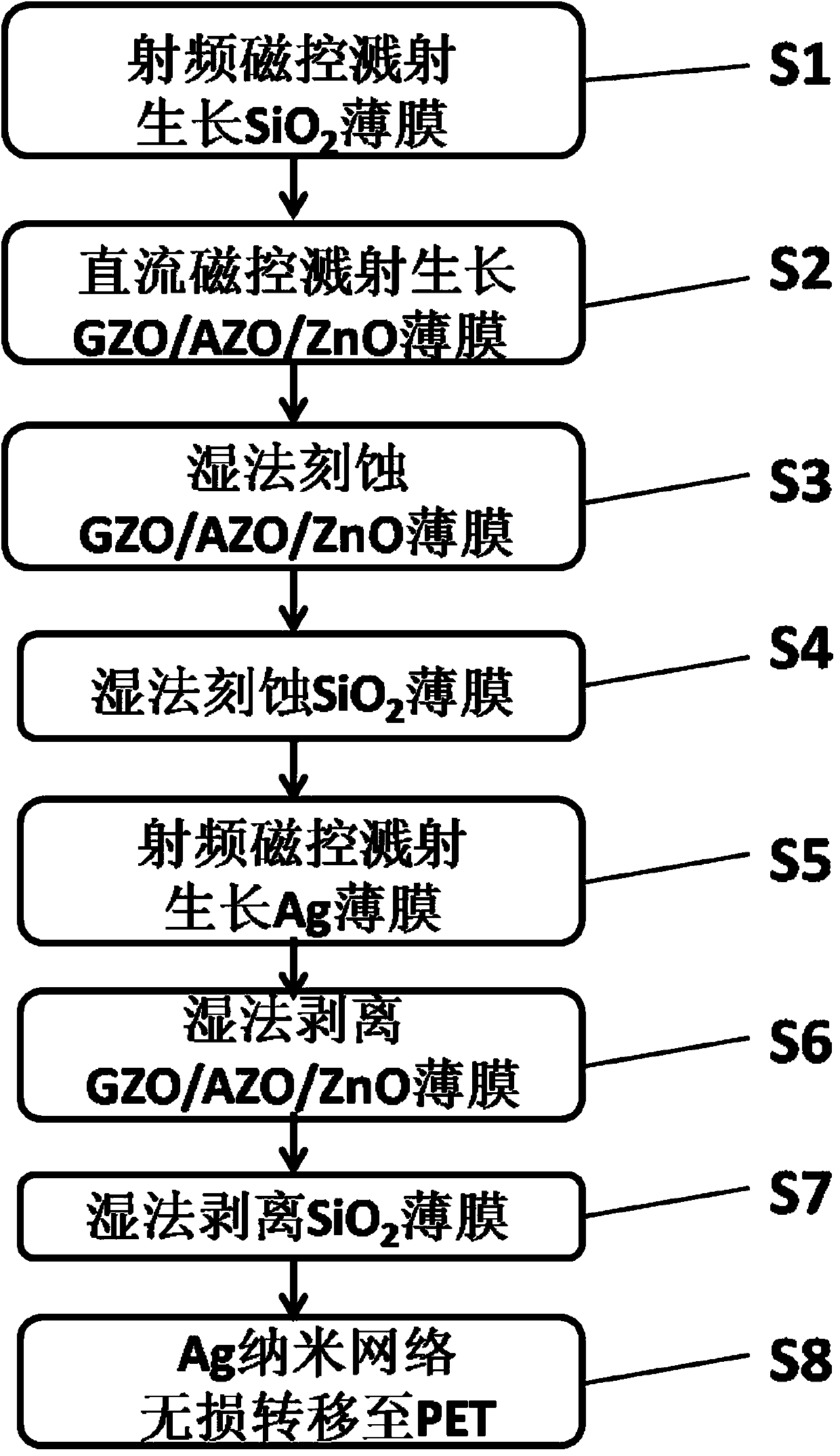
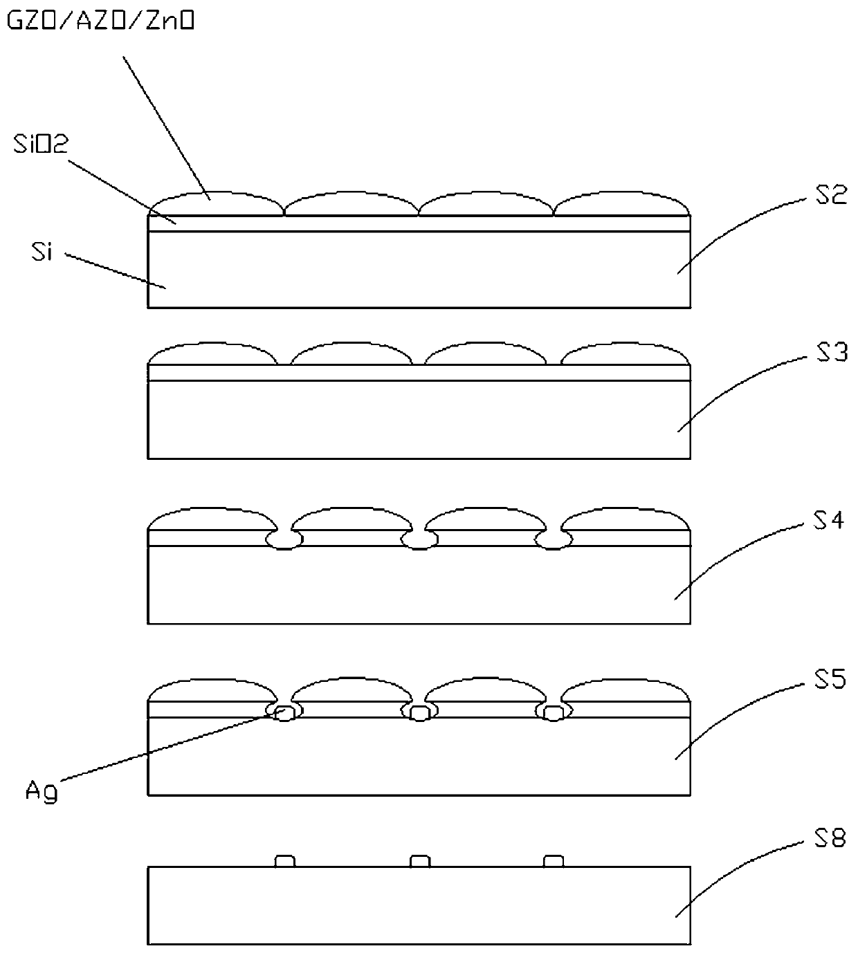
[0029] Such as figure 1 with figure 2 As shown, the method for preparing a metal nano-network flexible panel for electronic information display provided by the present invention includes the following steps:
[0030] S1, using silicon ceramic as the substrate, placing the substrate in the magnetron sputtering chamber, using Ar ion as the sputtering gas, O 2 As a reactive gas, the radio frequency power is applied to the cathode, and the preparation temperature is kept at room temperature; the sputtering power is 250W, the working pressure is 0.5Pa, the target voltage is 87V, the distance between the substrate and the target is 70mm, and SiO is prepared. 2 Sacrificial layer with a film thickness of 300 nm.
[0031] S2, using magnetron sputtering method, in SiO 2 GZO film is prepared on the film as a covering layer, GZO ceramic target is used, Ar ion is used as sputtering gas, DC power is applied to the cathode, the sputtering power is 300W, the working pressure is 0.2Pa, the target v...
Embodiment 2
[0040] The invention provides a method for preparing a metal nano-network flexible panel for electronic information display, including the following steps:
[0041] S1, using silicon ceramic as the substrate, placing the substrate in the magnetron sputtering chamber, using Ar ion as the sputtering gas, O 2 As a reactive gas, the radio frequency power is applied to the cathode, and the preparation temperature is kept at room temperature; the sputtering power is 250W, the working pressure is 0.5Pa, the target voltage is 87V, the distance between the substrate and the target is 70mm, and SiO is prepared. 2 Sacrificial layer with a film thickness of 300 nm.
[0042] S2, using magnetron sputtering method, in SiO 2 AZO film is prepared on the film as a covering layer, AZO ceramic target is used, Ar ion is used as sputtering gas, DC power is applied to the cathode, the sputtering power is 350W, the working pressure is 0.2Pa, the target voltage is 441V, and the flexible panel substrate is T...
Embodiment 3
[0051] The invention provides a method for preparing a metal nano-network flexible panel for electronic information display, including the following steps:
[0052] S1, using silicon ceramic as the substrate, placing the substrate in the magnetron sputtering chamber, using Ar ion as the sputtering gas, O 2 As a reactive gas, the radio frequency power is applied to the cathode, and the preparation temperature is kept at room temperature; the sputtering power is 250W, the working pressure is 0.5Pa, the target voltage is 87V, the distance between the substrate and the target is 70mm, and SiO is prepared. 2 Sacrificial layer with a film thickness of 300 nm.
[0053] S2, using magnetron sputtering method, in SiO 2 ZnO film is prepared on the film as a covering layer, ZnO ceramic target is used, Ar ion is used as sputtering gas, DC power is applied to the cathode, sputtering power is 400W, working pressure is 0.2Pa, target voltage is 468V, flexible panel substrate The pitch of the target ...
PUM
| Property | Measurement | Unit |
|---|---|---|
| thickness | aaaaa | aaaaa |
| thickness | aaaaa | aaaaa |
| electrical resistivity | aaaaa | aaaaa |
Abstract
Description
Claims
Application Information

