Semiconductor structure and formation method

A semiconductor and gate structure technology, applied in the field of semiconductor structure and its formation, can solve the problems that the electrical performance of semiconductor devices needs to be improved, and achieve the effects of avoiding adverse effects, improving controllability, and improving blocking effect

Active Publication Date: 2018-06-12
SEMICON MFG INT (SHANGHAI) CORP +1
View PDF5 Cites 1 Cited by
  • Summary
  • Abstract
  • Description
  • Claims
  • Application Information

AI Technical Summary

Problems solved by technology

[0004] Although the introduction of high-k metal gates can improve the electrical performance of semiconductor devices to a certain extent, the electrical performance of semiconductor devices formed by the prior art still needs to be improved.

Method used


Image

  • Semiconductor structure and formation method
  • Semiconductor structure and formation method
  • Semiconductor structure and formation method

Examples


Embodiment Construction

[0030] It can be seen from the background art that the electrical performance of semiconductor devices still needs to be improved. Combined with a method of forming a semiconductor structure, the reason is analyzed.

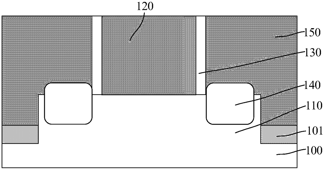
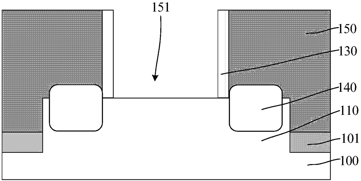
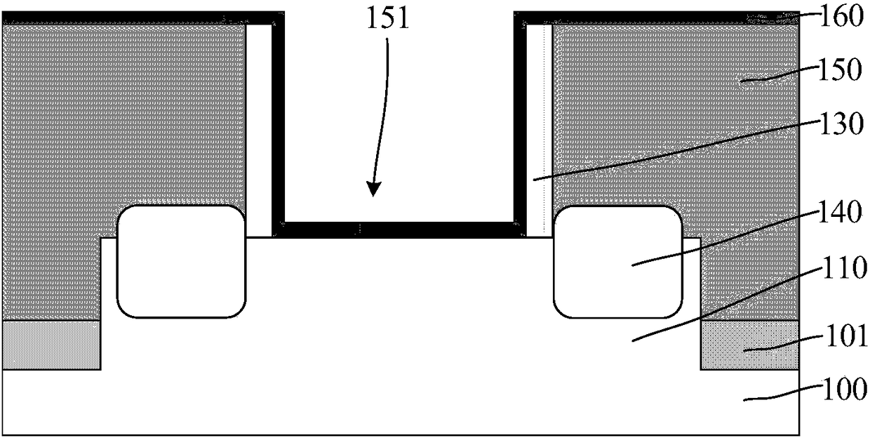
[0031] The forming method includes: providing a substrate; forming a gate dielectric layer on the substrate; forming a work function layer on the gate dielectric layer; forming a barrier layer on the work function layer; layer; the metal layer, the gate dielectric layer, the work function layer and the barrier layer are used to form a gate structure.

[0032] Wherein, the barrier layer is used to block easily diffusible ions (such as F ions) in the metal layer, and prevent the easily diffusible ions from diffusing into the work function layer, so that the formed semiconductor structure can be avoided. The problem of threshold voltage increase occurs; and the impact of the thickness of the barrier layer on the threshold voltage is more obvious, when the thickness...


PUM

PropertyMeasurementUnit
electron work functionaaaaaaaaaa

Abstract

A semiconductor structure and a formation method are disclosed. The method comprises the following steps of providing a substrate; forming a gate dielectric layer on the substrate; forming a work function layer on the gate dielectric layer; forming an oxide layer on the work function layer; forming a barrier layer on the oxide layer; and forming a metal layer on the barrier layer, wherein the metal layer, the gate dielectric layer, the work function layer, the oxide layer and the barrier layer are used for forming a gate structure. In the invention, the oxide layer is formed between the work function layer and the barrier layer; the oxide layer is a non-crystallizing film and a diffusion capability of diffusible ions in the metal layer is weak in the oxide layer so that the oxide layer canwell block diffusion of the diffusible ions into the work function layer, the work function value of the work function layer can be reduced and the threshold voltage of the formed semiconductor structure can be decreased. Compared with the scheme in which a barrier layer thickness is increased so as to improve a blocking effect, the oxide layer can prevent the increase of the thickness of the barrier layer from adversely affecting the electrical properties of a semiconductor device.

Description

technical field [0001] The invention relates to the field of semiconductors, in particular to a semiconductor structure and a forming method thereof. Background technique [0002] The main semiconductor device of an integrated circuit, especially a very large scale integrated circuit, is a metal-oxide-semiconductor field effect transistor (MOS transistor). With the continuous development of integrated circuit manufacturing technology, the technology nodes of semiconductor devices continue to decrease, and the geometric dimensions of semiconductor devices follow Moore's law. When the size of semiconductor devices is reduced to a certain extent, various secondary effects caused by the physical limits of semiconductor devices appear one after another, and it becomes more and more difficult to scale down the feature size of semiconductor devices. Among them, in the field of semiconductor manufacturing, the most challenging thing is how to solve the problem of large leakage curr...

Claims


Application Information

Patent Timeline
Patent Type & Authority Applications(China)
IPC IPC(8): H01L29/78H01L21/336
CPCH01L29/66795H01L29/785
Inventor 徐建华王安妮杨小军
Owner SEMICON MFG INT (SHANGHAI) CORP
Why Eureka
Try Eureka