Bipolar high-capacity organic field effect transistor memory and preparation method thereof

A large-capacity, organic field technology, applied in semiconductor/solid-state device manufacturing, electrical solid-state devices, semiconductor devices, etc., can solve the problem of only storing holes and electrons, and achieve lower threshold voltage and lower power consumption , The effect of simplifying the production process

Inactive Publication Date: 2018-06-12
NANJING UNIV OF POSTS & TELECOMM
View PDF4 Cites 8 Cited by
  • Summary
  • Abstract
  • Description
  • Claims
  • Application Information

AI Technical Summary

Problems solved by technology

However, most of the current organic field effect transistor memories are unipolar storage, which can only store holes or only store electrons.

Method used


Image

  • Bipolar high-capacity organic field effect transistor memory and preparation method thereof
  • Bipolar high-capacity organic field effect transistor memory and preparation method thereof
  • Bipolar high-capacity organic field effect transistor memory and preparation method thereof

Examples


Embodiment 1

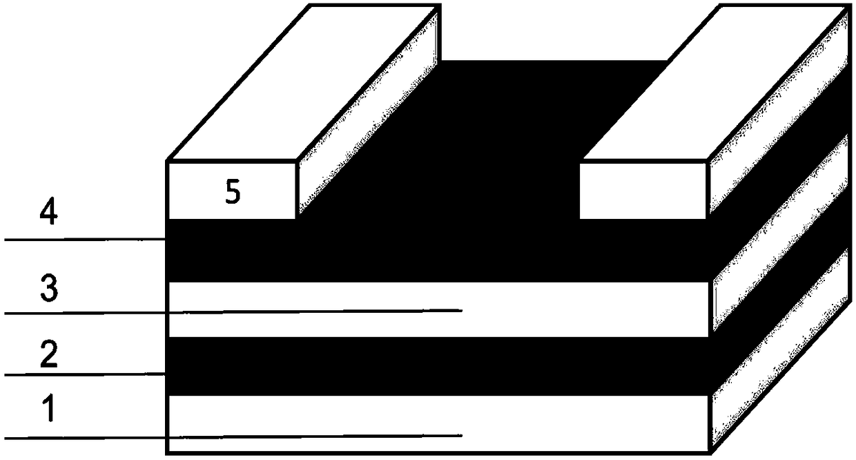
[0041] The structure diagram of the organic field effect transistor memory involved in the specific embodiment of the present invention is as follows: figure 1 As shown, a P-type and N-type semiconductor-doped nano-film as the OFET memory of the charge trapping layer includes a substrate, a gate electrode formed on the substrate, and a gate electrode covering the gate electrode from bottom to top. An insulating layer, a three-component doped organic nanometer floating gate layer spin-coated on the gate insulating layer, a semiconductor layer formed on the floating gate layer, and source and drain electrodes formed on both sides of the channel region on the upper surface of the semiconductor layer. In the technical scheme of the embodiment of the present invention, n-type heavily doped silicon is used as the gate; 300nm thick SiO is thermally evaporated on it 2 As a gate insulating layer; the charge trapping layer is made of polystyrene (PS) as a substrate, and the P-type semic...


PUM


Abstract

The invention discloses a bipolar high-capacity organic field effect transistor memory and a preparation method thereof. A series of P type and N type organic semiconductor materials are designed through band-gap engineering, a structure similar to an inorganic P-N junction is constructed through a solution spin-coating technology, and the problem of electron hole annihilation on the same wafer issolved, so that bipolar information storage of an electron hole is achieved. Meanwhile, due to a low threshold voltage, when the integrity is improved in the future, the power consumption and heatingare reduced, and information storage stability is achieved. The method aims to prepare a mixed nano-film with bipolar capture sites through simple solution spin-coating and achieve large-capacity bipolar storage. The preparation method of a film is beneficial to reduction of the production cost and large-area preparation in the low-temperature air environment.

Description

technical field [0001] The invention belongs to the technical field of semiconductor organic field effect transistor memory, and specifically relates to a floating gate type organic field effect transistor memory based on P-type organic semiconductor material and N-type organic semiconductor material through simple doping and a preparation method. Background technique [0002] Massive information calculation, storage, transmission and application have become the characteristics of the development of information electronic technology in the 21st century. Facing the advent of the big data era, massive data processing requires the development of large-capacity, high-density, and high-speed memories. Compared with traditional inorganic semiconductor memories, organic field-effect transistor memories have attracted much attention due to their natural advantages. Among them, the production cost of organic semiconductor materials is low, easy to obtain, can be processed by solution...

Claims


Application Information

Patent Timeline
Patent Type & Authority Applications(China)
IPC IPC(8): H01L51/05H01L51/30H01L51/40H01L27/28
CPCH10K19/10H10K71/12H10K85/60H10K85/615H10K10/462H10K10/466
Inventor 宋娟徐新水钱妍仪明东谢令海黄维
Owner NANJING UNIV OF POSTS & TELECOMM
Why Eureka
Try Eureka