Circular large-dimension IGBT chip crimping packaging structure and manufacturing method

A packaging structure and large-size technology, which is applied in semiconductor/solid-state device manufacturing, electrical components, electric solid-state devices, etc., can solve the problems of obvious influence of stray parameters, high assembly requirements, complicated operation, etc., and achieve simple operation and dual Surface heat dissipation and the effect of electrical connection

Active Publication Date: 2018-06-15
HUNAN UNIV
View PDF4 Cites 10 Cited by
  • Summary
  • Abstract
  • Description
  • Claims
  • Application Information

AI Technical Summary

Problems solved by technology

[0008] The purpose of the present invention is to address the above problems, to provide a circular large-size IGBT chip crimping package structure and manufacturing method, to solve the existing IGBT crimping package structure needs to cut the chips on the entire w

Method used


Image

  • Circular large-dimension IGBT chip crimping packaging structure and manufacturing method
  • Circular large-dimension IGBT chip crimping packaging structure and manufacturing method
  • Circular large-dimension IGBT chip crimping packaging structure and manufacturing method

Examples


Embodiment Construction

[0036] In order to enable those skilled in the art to better understand the technical solution of the present invention, the present invention will be described in detail below in conjunction with the accompanying drawings. The description in this part is only exemplary and explanatory, and should not have any limiting effect on the protection scope of the present invention. .

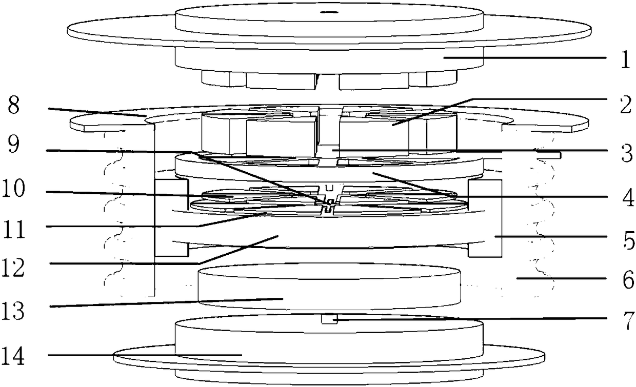
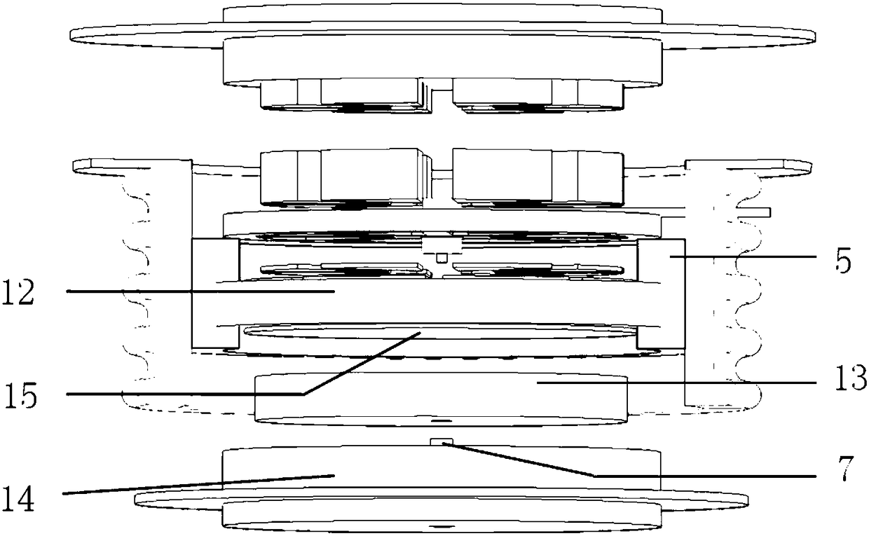
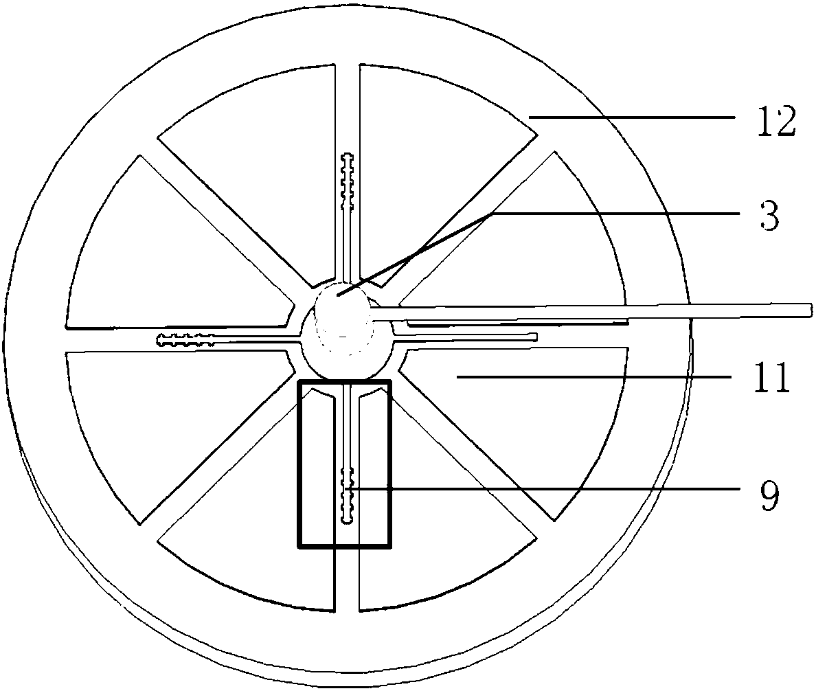
[0037] Such as figure 1 and figure 2 As shown, this embodiment provides a circular large-size IGBT chip crimp package structure, which includes an emitter terminal cover 1, an emitter molybdenum sheet 2, a gate pogo pin assembly 3, and a grid Metal 9, emitter molybdenum sheet positioning frame 4, soft conductive metal sheet 10, emitter metal 11, IGBT chip 12, collector metal 14, collector molybdenum sheet with positioning hole 13, positioning pin 7, collector end cover 14, Apron 5, metal skirt 8 and ceramic shell 6.

[0038] The top surface of the IGBT chip 12 is provided with an emitter metal laye...


PUM


Abstract

The invention discloses a circular large-dimension IGBT chip crimping packaging structure and a manufacturing method. The circular large-dimension IGBT chip crimping packaging structure comprises an emitting electrode end cover, emitting electrode molybdenum sheets, a gate spring needle assembly, gate metal, an emitting electrode molybdenum sheet positioning frame, flexible conductive metal thin sheets, emitting electrode metal, an IGBT chip, collector electrode metal, collector electrode molybdenum sheets with positioning holes, a collector electrode end cover and the like which are arrangedfrom the top to bottom in sequence. By adopting the crimping packaging structure, a fault sector region isolation method is simple, so that only the fault region sector conductive molybdenum sheets need to be changed into insulating sheets, and the gate metal specific connecting position on the surface of the chip is cut off; a device is subjected to two-sided heat dissipation through the collector electrode end cover and the emitting electrode end cover; metal bonding wires and a welding interface are omitted, so that the bottleneck of conventional device bonding point and welding layer fatigue failure can be eliminated, and relatively high resistance to thermal mechanical fatigue can be achieved; the interior of the device adopts symmetrical structural design, so that stray inductance ofeach sector region in the interior can be lowered, the stray inductance distribution can be consistent, the parasitic parameter of a module can be reduced, and the electrical performance of the device can be improved.

Description

technical field [0001] The invention relates to the field of semiconductor manufacturing, in particular to a circular large-size IGBT chip crimping package structure and a manufacturing method thereof. Background technique [0002] Insulated Gate Bipolar Transistor (IGBT) is a power electronic device that combines the advantages of metal-oxide-semiconductor field-effect transistors (MOSFET) and bipolar junction transistors. IGBT is known for its excellent performance It has been widely used and greatly improved the performance of power electronic devices and systems. [0003] With the continuous expansion of the application field, the performance requirements for IGBT devices are getting higher and higher, and the existing technology has the following defects: 1. On the one hand, it is required to increase the power level of the device, and the traction of high-power electric locomotives, power transmission and transformation systems , new energy, national defense heavy ind...

Claims


Application Information

Patent Timeline
IPC IPC(8): H01L29/739H01L23/04H01L23/20H01L23/367H01L21/52H01L21/54
CPCH01L21/52H01L21/54H01L23/041H01L23/20H01L23/367H01L29/7395
Inventor 王俊李锋曾重
Owner HUNAN UNIV
Why Eureka
Try Eureka