Check patentability & draft patents in minutes with Patsnap Eureka AI!

High-speed CMOS transmission gate switch circuit

A switching circuit and transmission gate technology, applied in the field of high-speed CMOS transmission gate switching circuit, can solve the problems of increasing signal load, excessive conduction resistance, limiting signal transmission speed, etc. Effects of drive voltage, increased bandwidth, and linearity

Active Publication Date: 2018-06-22
TSINGHUA UNIV
View PDF4 Cites 3 Cited by
  • Summary
  • Abstract
  • Description
  • Claims
  • Application Information

AI Technical Summary

Problems solved by technology

For high-speed systems, the large on-resistance will limit the signal transmission bandwidth, thereby limiting the signal transmission speed
Generally, if the on-resistance near Vcm is too large, a MOS transistor with a large W / L (width-to-length ratio) will be used, which will not only increase the signal load, but also a large load for the clock.
[0007] Second: The switch on-resistance varies greatly across the input range
from image 3 It can be seen from the solid line of , that for different input voltages Vin, the on-resistance is small at both ends and large in the middle, which will lead to nonlinear signal transmission and affect the accuracy of the system
[0008] Therefore, the traditional CMOS transmission gate switching circuit needs to be further improved in terms of speed and accuracy.

Method used


Image

  • High-speed CMOS transmission gate switch circuit
  • High-speed CMOS transmission gate switch circuit
  • High-speed CMOS transmission gate switch circuit

Examples


Embodiment Construction

[0019] In order to make the object, technical solution and advantages of the present invention clearer, the implementation of the present invention will be further described in detail below in conjunction with the accompanying drawings.

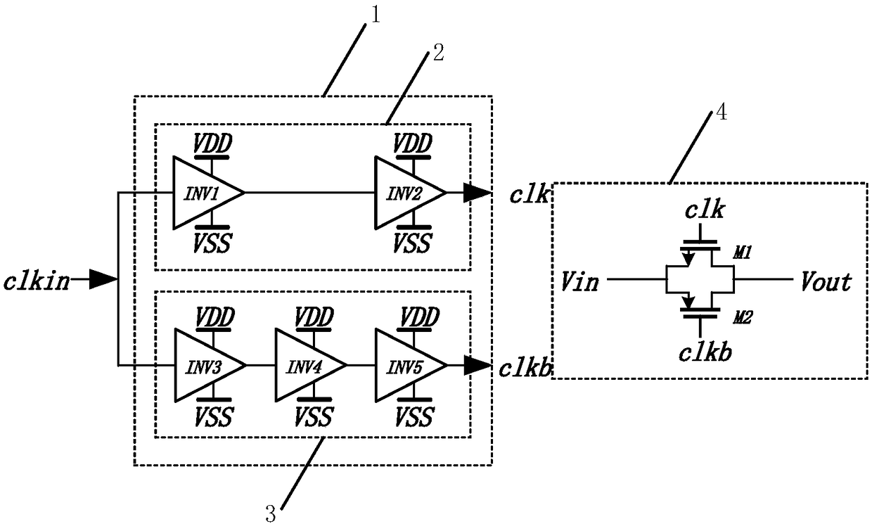
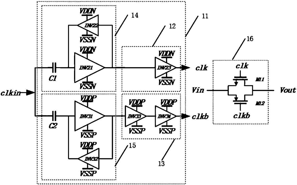
[0020] The structure of the CMOS transmission gate switch circuit of the embodiment of the present invention is as follows figure 2 As shown, the circuit includes:

[0021] The clock control circuit 11 with level shifting includes two sub-channels, the signal input terminals of the two sub-channels are connected to the clock signal clkin at the same time; the first sub-channel is used to make the input voltage amplitude between [VDD, VSS] The clock signal clkin Shift up to become the same-phase clock signal clk with a voltage amplitude between [VDDN, VSSN], which is output from the signal output terminal of the first sub-channel; the second sub-channel is used to make the input voltage amplitude between [VDD, VSS] The clock signal clkin bet...


PUM


Abstract

The invention provides a high-speed CMOS (Complementary Metal Oxide Semiconductor) transmission gate switch circuit, belonging to the technical field of transmission gate circuit design. The switch circuit comprises a CMOS transmission gate composed of an NMOS (N-type Metal Oxide Semiconductor) transistor and a PMOS (P-type Metal Oxide Semiconductor) transistor that are complementary, and a clockcontrol circuit composed of two sub-channels and having a level shifting function; the first sub-channel is used for generating an in-phase clock control signal for integrally shifting the level of aninput clock signal up, and the output end of the first sub-channel is connected to a gate of the NMOS transistor; the second sub-channel is used for generating an inverted clock control signal for integrally shifting the level of the input clock signal down, and the second sub-channel output is connected to a gate of the PMOS transistor. When the switch circuit is turned on, the overdrive voltageof the NMOS and PMOS transistors is increased, the on-resistance is reduced, the signal transmission speed is improved, and the nonlinear problem of the on-resistance changing with the change of input is reduced at the same time, so that the switch circuit can be applied to a circuit system having high speed and high precision requirements.

Description

technical field [0001] The invention belongs to the technical field of transmission gate circuit design, in particular to a high-speed CMOS transmission gate switch circuit. Background technique [0002] The switched capacitor circuit is an important circuit in the analog circuit, which can be used to implement switched capacitor filters, capacitive sample-and-hold devices, switched capacitor amplifiers, and switched capacitor analog-to-digital converters (ADC), etc. The switch circuit is an important part of the switched capacitor circuit. Through the on and off of the switch circuit, the transfer of the capacitor charge is realized, thereby realizing the maintenance and amplification of the voltage. [0003] There are many ways to realize the switch circuit. A separate NMOS transistor or a separate PMOS transistor can be used to control the gate voltage of the NMOS transistor or PMOS transistor to realize the on and off of the switch, but using a separate NMOS transistor o...

Claims


Application Information

Patent Timeline
IPC IPC(8): H03K17/06H03K17/687
CPCH03K17/06H03K17/687
Inventor 李福乐刘佳
Owner TSINGHUA UNIV
Features
  • R&D
  • Intellectual Property
  • Life Sciences
  • Materials
  • Tech Scout
  • Unparalleled Data Quality
  • Higher Quality Content
  • 60% Fewer Hallucinations
Learn More