

Design and manufacture method of millimeter wave 3D coaxial transmission line
A technology for coaxial transmission lines and manufacturing methods, applied in waveguides, waveguide-type devices, circuits, etc., can solve the problems of difficult high-reliability millimeter-wave coaxial transmission lines, high processing costs, and low reliability
- Summary
- Abstract
- Description
- Claims
- Application Information
AI Technical Summary
Problems solved by technology
Method used
Image

Examples
Embodiment 1
[0048] Embodiment 1: a 3D transmission line with an upper limit of operating frequency of 150 GHz and an impedance of 50 ohm.
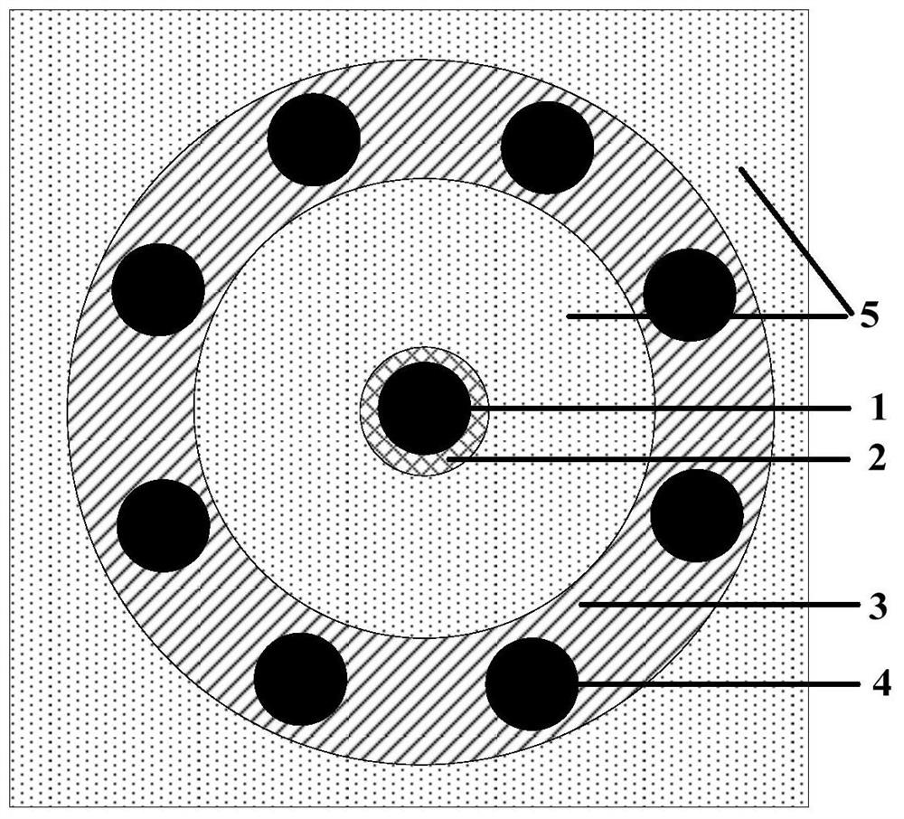
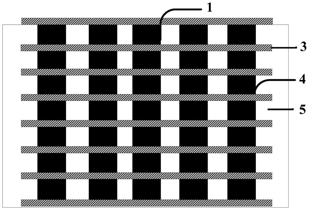
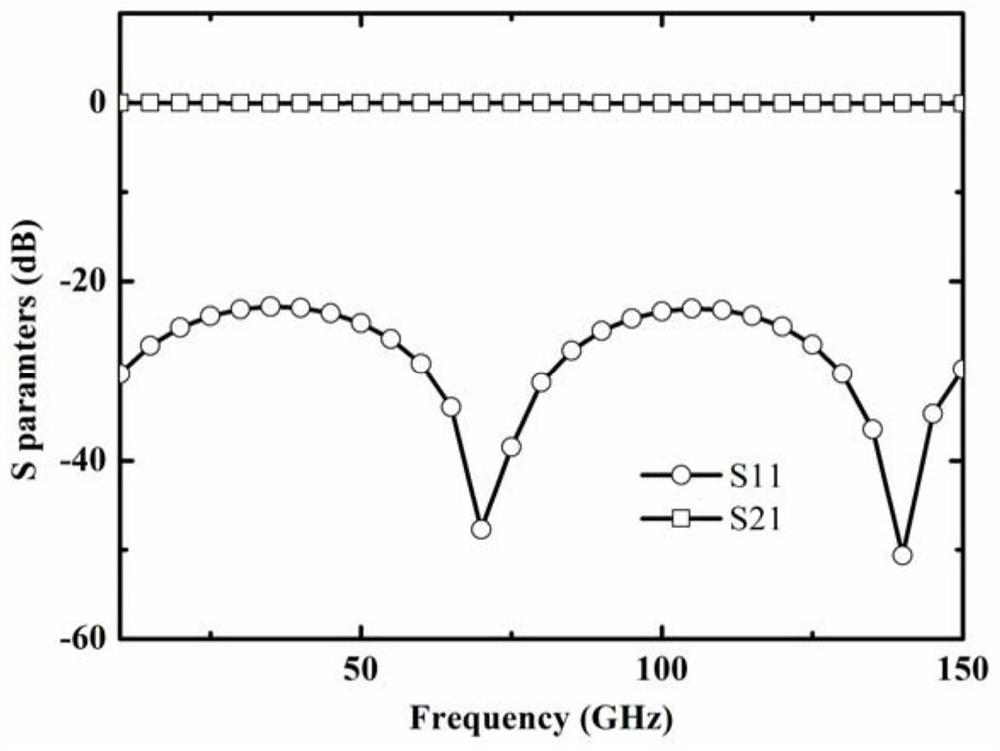
[0049] Select the diameter of the central conductor post 1 to be 100 μm, the diameter of the protective pad 2 of the central conductor post to be 150 μm; the diameter of the cylindrical ground via post 4 to be 100 μm, and the distance from the center of the central conductor post 1 to be 480 μm, the inner diameter of the annular protective pad 3 is 760 μm, and the outer diameter is 960 μm; the relative dielectric constant of the Ferro A6M ceramic dielectric material used is 5.9, the single-layer height of the ceramic after sintering is 96 μm, and the number of layers of the ceramic used is 9 floors. The simulated two-port S-parameter curve is as follows image 3 shown.
Embodiment 2
[0050] Embodiment 2: a transmission line with an upper limit of operating frequency of 300 GHz and an impedance of 50 ohm. The diameter of the cylindrical grounding via column is 100 μm, the distance from the center of the central conductor column 1 is 700 μm, the inner diameter of the annular protection pad 3 is 625 μm, and the outer diameter is 775 μm; Ferro A6M ceramics are used The dielectric constant of the dielectric material is 5.9, the height of the sintered single-layer ceramic is 96 μm, and the number of layers of the ceramic used is 9. The simulated two-port S-parameter curve is as follows Figure 4 shown.
[0051] The present invention is superior to the prior art solutions in that: Ferro A6M material with lower millimeter wave loss is used as the substrate; laser alignment technology is used to ensure the positioning accuracy after stacking and sintering; laser drilling technology is used to obtain the desired accurate metal pass. The shape of the hole and the s...
PUM
| Property | Measurement | Unit |
|---|---|---|
| height | aaaaa | aaaaa |
| relative permittivity | aaaaa | aaaaa |
Abstract
Description
Claims
Application Information