Silicon wafer processing device

A processing device and silicon crystal technology, applied in the direction of fine working devices, stone processing equipment, working accessories, etc., can solve the problems of low equipment utilization, high production and use costs, single function, etc., to achieve high clamping efficiency and reduce Cost of production and use, simple effect of switching

Active Publication Date: 2018-07-10
福州天瑞线锯科技有限公司
View PDF9 Cites 15 Cited by
  • Summary
  • Abstract
  • Description
  • Claims
  • Application Information

AI Technical Summary

Problems solved by technology

[0004] Therefore, it is necessary to provide a silicon crystal processing device to solve the problems of single application function, low equipment utilization rate and high production and use cost of the existing silicon crystal processing device

Method used


Image

  • Silicon wafer processing device
  • Silicon wafer processing device
  • Silicon wafer processing device

Examples


Embodiment Construction

[0051] In order to describe in detail the technical content, structural features, achieved objectives and effects of the technical solution, the following detailed descriptions are given in conjunction with specific embodiments and accompanying drawings.

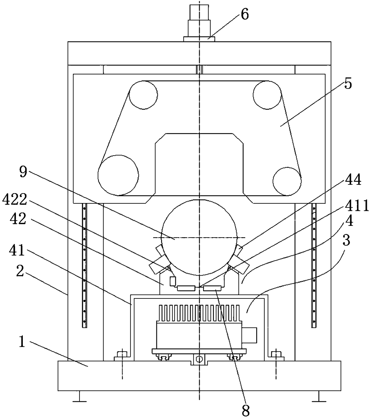
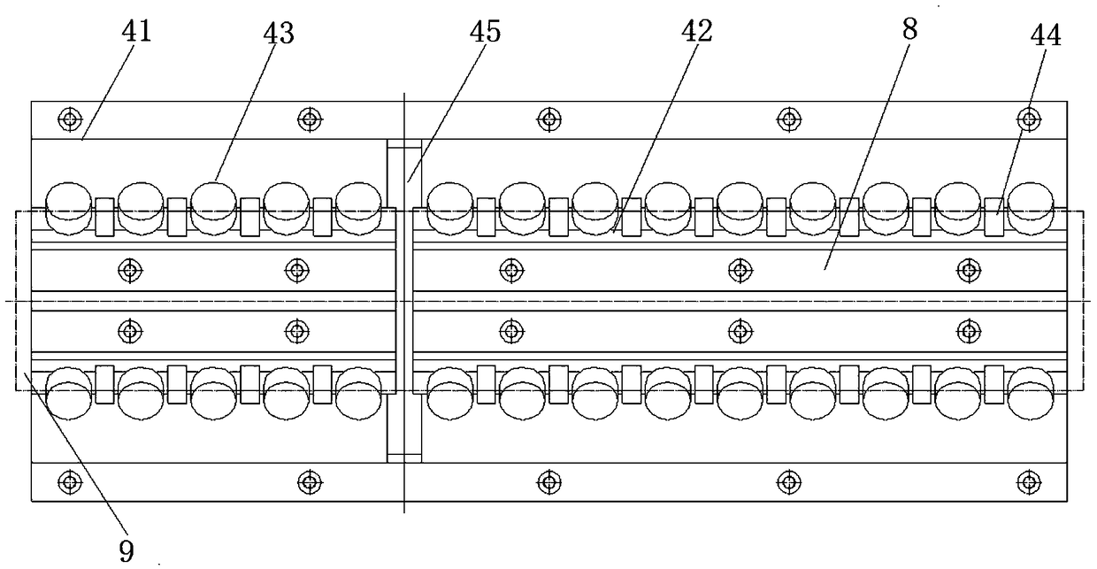
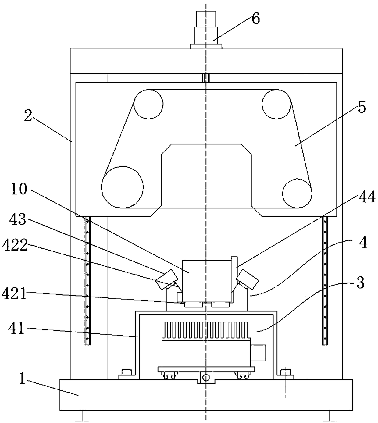
[0052] See Figure 1 to Figure 6 , The present invention provides a silicon crystal processing device, the processing device includes a base 1, a frame 2, a square opening and clamping mechanism 3, a silicon crystal cutting and clamping mechanism 4, and a wire saw cutting machine 5; the frame 2 Set on the base 1; the base 1 and the bracket fixed on the base 1 are used as the main structure of the silicon crystal processing device of the present invention to carry and fix other components, such as: square clamping mechanism 3, wire saw cutting machine 5 Wait.

[0053] The square rooting and clamping mechanism 3 is used to load and fix the seed crystal rods to be square rooted. The specific structure is as follows: the square ope...


PUM


Abstract

The invention relates to a silicon wafer processing device. The silicon wafer processing device comprises a base, a rack, a squaring clamping mechanism, a silicon wafer cut-off clamping mechanism anda wire saw cutting machine, wherein the squaring clamping mechanism is used for clamping to-be-squared seed crystal rods, the silicon wafer cut-off clamping mechanism is used for clamping single-crystal silicon rods or polycrystalline silicon blocks to be cut-off, and the wire saw cutting machine is used for squaring the seed crystal rods and cutting off the single-crystal silicon rods or the polycrystalline silicon blocks. The silicon wafer processing device integrates the silicon wafer squaring and cut-off functions, not only can achieve squaring of the seed crystal rods, but also can achieve cutting off or slicing of the single-crystal silicon rods or the polycrystalline silicon blocks, the structure is simple and compact, the production cost and using cost of manufacturers are reduced,and the equipment utilization rate is increased.

Description

Technical field [0001] The invention relates to the technical field of cutting hard and brittle materials, in particular to a silicon crystal processing device. Background technique [0002] Silicon crystals are widely used in the photovoltaic industry. In order to meet the quality parameters of the silicon ingot and the shape and size of the next process, the preliminary processing of the silicon rod is an indispensable step in the preliminary process of photovoltaic solar cells. First, the seed crystal needs to be processed, the seed crystal is squared, and then the single crystal silicon rod is drawn through the seed crystal, or the polycrystalline silicon block is cast, and then the single crystal silicon rod and polycrystalline silicon block are truncated and sliced. From the perspective of the cutting process, whether it is a long-wire diamond wire or a ring diamond wire saw, the cutting process parameters for seed crystals, cylindrical monocrystalline silicon rods, and cu...

Claims


Application Information

Patent Timeline
Patent Type & Authority Applications(China)
IPC IPC(8): B28D5/04B28D7/04B28D7/00
CPCB28D5/0058B28D5/0082B28D5/04
Inventor 朱文志李海威林冬黄田玉林孝狮许光先梁兴华林光展
Owner 福州天瑞线锯科技有限公司
Why Eureka
Try Eureka