

Alkali halide-doped perovskite light-emitting diode and fabrication method thereof
A technology of alkali metal halides and light-emitting diodes, applied in semiconductor/solid-state device manufacturing, electrical components, electric solid-state devices, etc., can solve problems such as slow charge transfer efficiency, improve film morphology, improve device efficiency, and reduce costs Effect
- Summary
- Abstract
- Description
- Claims
- Application Information
AI Technical Summary
Problems solved by technology
Method used
Image

Examples
Embodiment 1
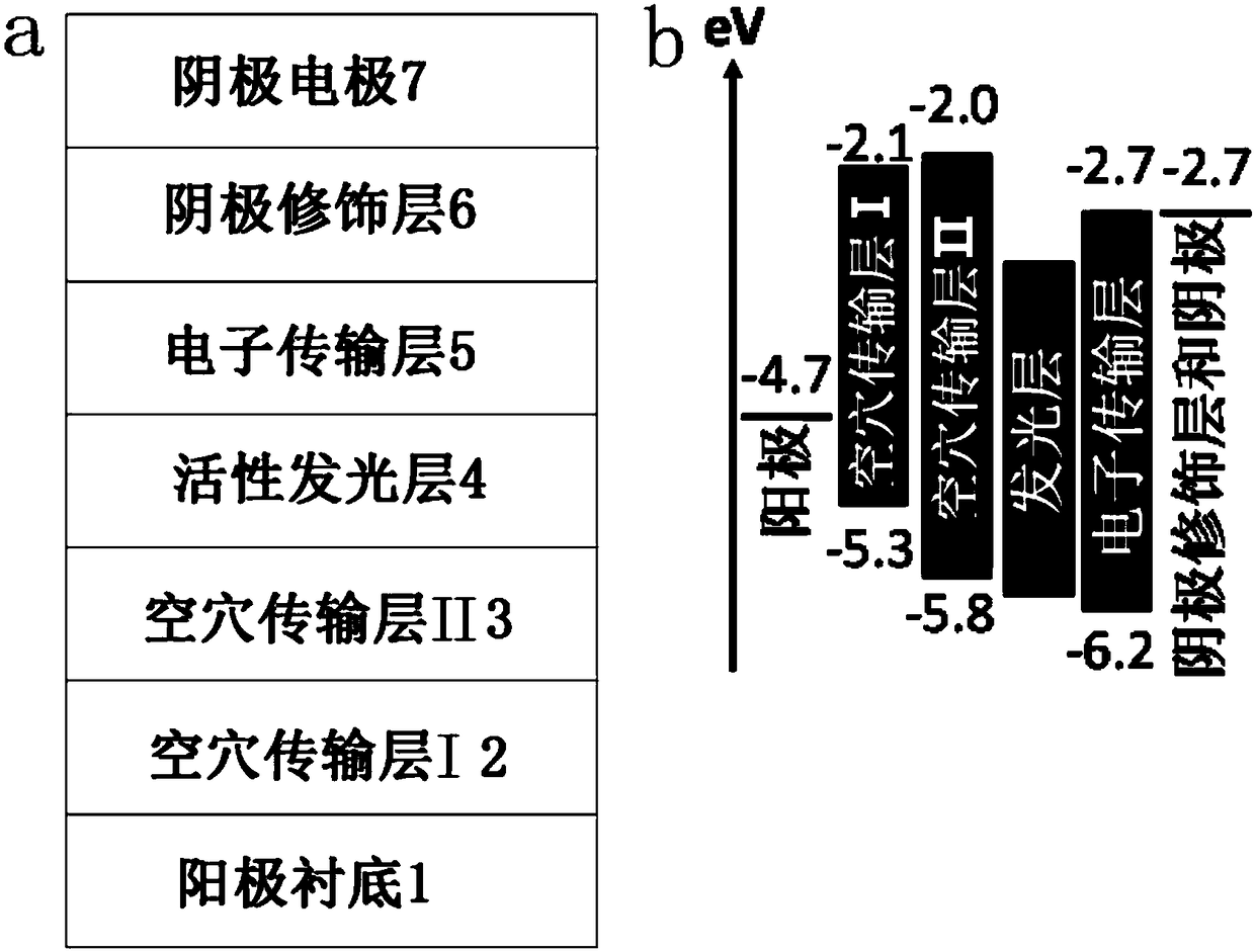
[0069] This embodiment provides an alkali metal halide-doped perovskite light-emitting diode, including an anode substrate 1 (thickness is 150nm), a hole transport layer (thickness is 40nm), an active light emitting diode arranged in sequence from bottom to top. Layer 4 (thickness is 40nm), electron transport layer 5 (thickness is 40nm), cathode modification layer 6 (thickness is 1nm) and cathode 7 (thickness is 100nm), wherein the hole transport layer comprises hole transport layer I 2 and hole Hole transport layer II 3. Its preparation method is as follows:
[0070] Using dimethyl sulfoxide (DMSO) as solvent to prepare perovskite precursor solution doped with alkali metal bromide, including perovskite precursors CsBr and PbBr 2 And the alkali metal bromide NaBr, the molar ratio of the three is CsBr:NaBr:PbBr 2 =1:0.1:1, CsBr and PbBr in the precursor solution 2 The optimal concentration is 0.2M, and the concentration of NaBr is 0.1M.
[0071] Dissolve TFB in chlorobenzen...
Embodiment 2
[0080] This embodiment provides an alkali metal halide-doped perovskite light-emitting diode, including an anode substrate 1 (thickness is 150nm), a hole transport layer (thickness is 40nm), an active light emitting diode arranged in sequence from bottom to top. Layer 4 (thickness is 40nm), electron transport layer 5 (thickness is 40nm), cathode modification layer 6 (thickness is 1nm) and cathode 7 (thickness is 100nm), wherein the hole transport layer comprises hole transport layer I 2 and hole Hole transport layer II 3. Its preparation method is as follows:
[0081] Using dimethyl sulfoxide (DMSO) as solvent to prepare perovskite precursor solution doped with alkali metal bromide, including perovskite precursors CsBr and PbBr 2 And the alkali metal bromide KBr, the molar ratio of the three is CsBr:KBr:PbBr 2 =1:0.1:1, precursor solution CsBr and PbBr 2 The optimal concentration is 0.2M, and the concentration of KBr is 0.1M.
[0082] Dissolve TFB in chlorobenzene to confi...
Embodiment 3
[0090] This embodiment provides an alkali metal halide-doped perovskite light-emitting diode, including an anode substrate 1 (thickness is 150nm), a hole transport layer (thickness is 40nm), an active light emitting diode arranged in sequence from bottom to top. Layer 4 (thickness is 40nm), electron transport layer 5 (thickness is 40nm), cathode modification layer 6 (thickness is 1nm) and cathode 7 (thickness is 100nm), wherein the hole transport layer comprises hole transport layer I 2 and hole Hole transport layer II 3. Its preparation method is as follows:
[0091] Using dimethyl sulfoxide (DMSO) as solvent to prepare perovskite precursor solution doped with alkali metal bromide, including perovskite precursors CsBr and PbBr 2 And the alkali metal bromide RbBr, the molar ratio of the three is CsBr:RbBr:PbBr 2 = 1:0.1:1, CsBr and PbBr 2 The optimal concentration is 0.2M, and the concentration of RbBr is 0.1M.
[0092] Dissolve TFB in chlorobenzene to configure a precurso...
PUM
 Abstract
Description
Claims
Application Information