Film mask, method for manufacturing same, and method for forming pattern using film mask and pattern formed thereby
A mask and pattern technology, applied to the originals for photomechanical processing, photosensitive materials for photomechanical equipment, photomechanical equipment, etc., can solve problems such as roller deformation, and achieve the effect of reducing unevenness
- Summary
- Abstract
- Description
- Claims
- Application Information
AI Technical Summary
Problems solved by technology
Method used
Image
Examples
preparation example Construction
[0073] Still another exemplary embodiment of the present specification provides a method of manufacturing a film mask, the method of manufacturing including:
[0074] forming a darkened light-shielding pattern layer on the transparent substrate; and
[0075] A relief pattern portion is formed on the surface of the transparent substrate provided with the darkened light-shielding pattern layer.
[0076] The formation of the darkened light-shielding pattern layer can be performed by forming a darkened light-shielding layer on a transparent substrate using a material for forming a darkening light-shielding pattern layer, and then performing photoresist (PR) coating, ultraviolet exposure, development, etching and stripping process. Said steps can go through a verification and repair process as needed.
[0077] Formation of the embossed pattern portion may be performed by a process of applying an adhesive resin and exposing to ultraviolet rays, and then applying and exposing a res...
Embodiment 1
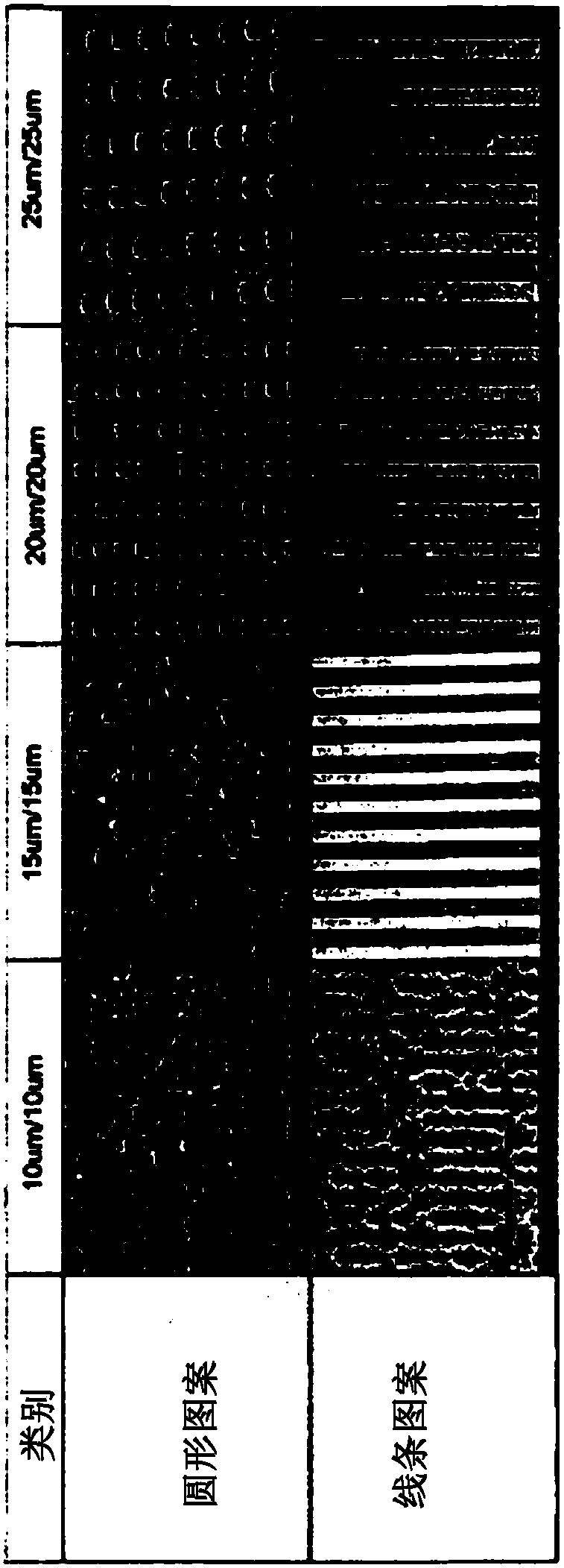
[0084] A urethane-based material was used to form an adhesion layer on a PET substrate with a thickness of 250 μm, plasma pretreatment was performed, and then an Al layer with a thickness of 100 nm was formed by sputtering. An AlOxNy layer (x>0 and 0.3≤y≤1) is formed by reactive sputtering by adding reactive gas nitrogen on the Al layer. Subsequently, a positive photoresist (manufactured by DongJinSemichem Co., Ltd., N200) was coated and fixed on a stage, and UV exposure was performed using a UV laser with a wavelength of 365 nm. Subsequently, a photoresist pattern was formed by developing using a 1.38% TMAH solution. Using the photoresist pattern, the Al layer and the AlOxNy layer were etched using an acid solution, and stripped using a stripping solution (LG Chem., LG202) to form a pattern. At this time, the openings of the AlOxNy layer were designed so that the pitch of the dot pattern with a diameter of 15 μm was 115 μm.
[0085] Subsequently, an adhesive layer was coate...
PUM
| Property | Measurement | Unit |
|---|---|---|
| reflectivity | aaaaa | aaaaa |
| diameter | aaaaa | aaaaa |
| width | aaaaa | aaaaa |
Abstract
Description
Claims
Application Information


