Display panel, manufacturing method thereof and display device

A technology for a display panel and a manufacturing method, applied in the field of display panels and display devices, capable of solving problems such as planarization layer damage and poor display performance, achieving the effects of uniform thickness, avoiding poor display performance, and optimizing process methods

Active Publication Date: 2018-08-03
KUNSHAN GO VISIONOX OPTO ELECTRONICS CO LTD
View PDF4 Cites 3 Cited by
  • Summary
  • Abstract
  • Description
  • Claims
  • Application Information

AI Technical Summary

Problems solved by technology

[0005] Embodiments of the present application provide a display panel, a manufacturing method thereof, and a display device to solve the problem of poor display performance due to damage to the planarization layer during anodic etching

Method used


Image

  • Display panel, manufacturing method thereof and display device
  • Display panel, manufacturing method thereof and display device
  • Display panel, manufacturing method thereof and display device

Examples


Embodiment 1

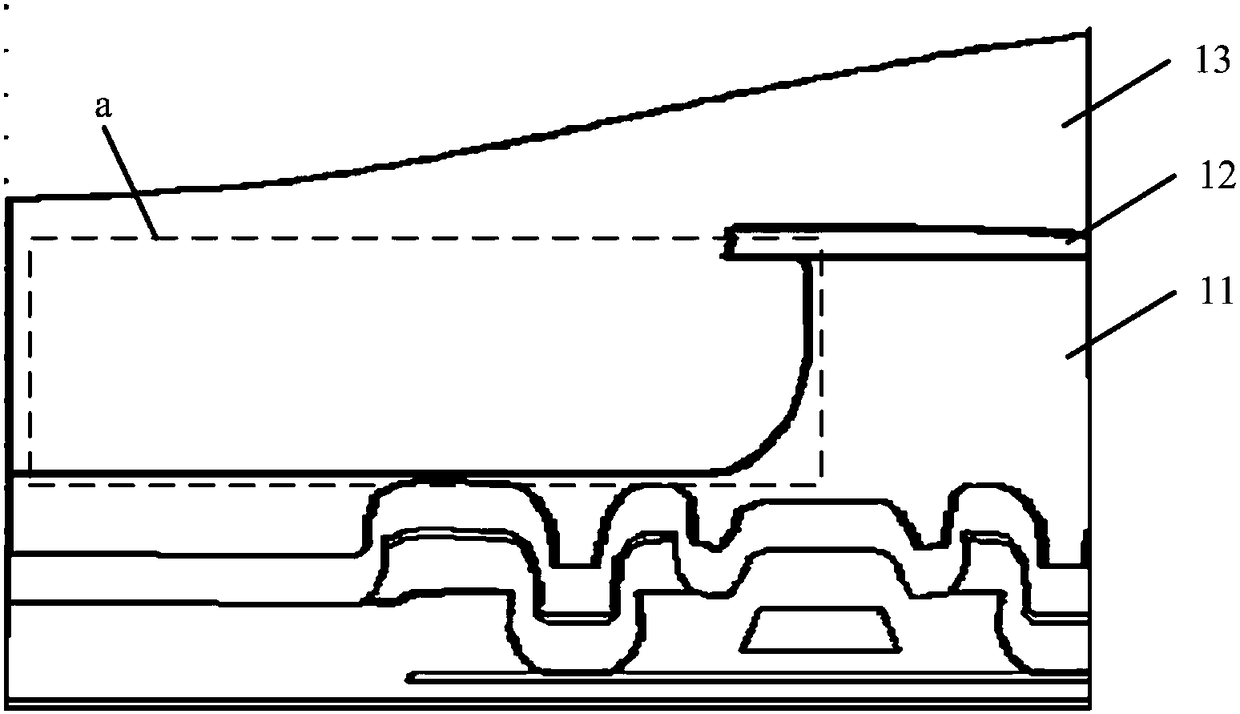
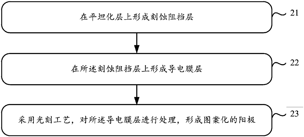
[0041] The embodiment of the present application provides a method for manufacturing a display panel, the flow chart of the method is as follows figure 2 As shown, the method is used to solve the problem that the planarization layer is damaged during the anode etching process, resulting in poor display performance. The aforementioned poor display performance is mainly due to the fact that the planarization layer is damaged during the anode etching process, so that the overall thickness of the pixel definition layer formed on the planarization layer is uneven. Subsequently, in the process of evaporating the light-emitting layer, there is a gap between the mask plate and the pixel definition layer covered by the mask plate, so that the light-emitting layer is also evaporated in the pixel definition layer at the position covered by the mask plate, resulting in inaccurate evaporation positions of the light-emitting layer. Affects the luminous effect of the emissive layer. The me...

Embodiment 2

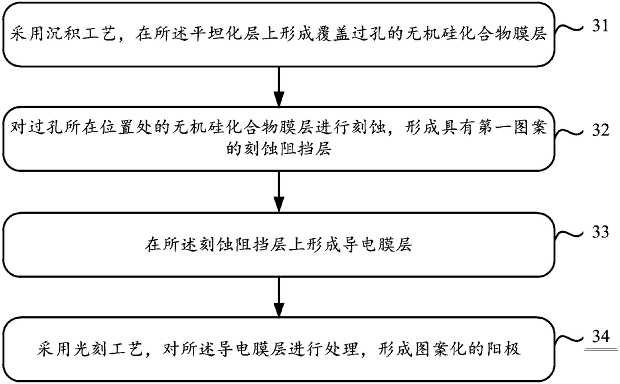
[0052] Based on the above-mentioned embodiments, this embodiment provides a better method for manufacturing a display panel. The process of the method is as follows: image 3 shown, including the following steps:

[0053] Step 31: Using a deposition process, forming an inorganic silicon compound film layer covering the via holes on the planarization layer;

[0054] Specifically, the material of the inorganic silicon compound film layer can be silicon oxide or silicon nitride, and the film layer can be deposited on the planarization layer by means of low-temperature chemical vapor deposition, which can cover the planarization layer and the transition layer in the planarization layer. hole location.

[0055] Step 32: Etching the inorganic silicon compound film layer at the position of the via hole to form an etching stopper layer having a first pattern.

[0056] Since the inorganic silicon compound film layer does not have good electrical conductivity and covers the via hole p...

Embodiment 3

[0065] Based on the above-mentioned embodiments, this embodiment provides another preferred method for manufacturing a display panel. The flow of the method is as follows: Figure 4 shown, including the following steps:

[0066] Step 41: Using a deposition process, forming a metal film layer covering the via holes on the planarization layer as an etching stopper layer.

[0067] Specifically, the material of the metal film layer may be an inert metal such as titanium or molybdenum, and the film layer may be deposited on the planarization layer by physical vapor deposition, which can cover the planarization layer and the positions of via holes in the planarization layer.

[0068] Since the metal film layer has a certain conductivity, the metal film layer covering the via hole will not significantly affect the signal transmission between the transmission line under the planarization layer and the anode layer. Therefore, there is no need to modify the position of the via hole The...


PUM


Abstract

The invention relates to the field of display, and in particular relates to a display panel, a manufacturing method thereof and a display device. The problem that a planarization layer is destroyed inan anode etching process in the prior art is solved. According to the structure of the display panel, an etch barrier layer is formed on the planarization layer; a conductive film layer is formed onthe etch barrier layer; the conductive film layer is processed by a photolithography process to form a patterned anode; and the etch barrier layer is used to prevent the planarization layer from beingcorroded by an ashing material used when the patterned anode is formed. According to the technical scheme provided by the invention, the planarization layer is protected by the etch barrier layer; the planarization layer is prevented from being corroded by the ashing material used when the anode is etched during the anode etching process; and the problems of inaccurate position of a evaporation luminescent layer and poor display performance, which are caused by uneven thickness of a pixel defining layer formed on the planarization layer, are prevented.

Description

technical field [0001] The present application relates to the field of display technology, and in particular to a display panel, a manufacturing method thereof, and a display device. Background technique [0002] In the field of display technology, the display layer structure such as figure 1 As shown, it should be noted that, figure 1 It only shows the position and relationship of the film layers, and does not reflect the actual film thickness. The actual film thickness can be adjusted according to the actual needs of production. The above-mentioned display layer includes film layers such as a planarization layer 11, an anode 12, and a pixel definition layer 13, wherein the anode 12 can be made of indium tin oxide (ITO) and aluminum (Al) to form a laminated structure of ITO and Al, wherein Al It is located between the ITO and the planarization layer 11 . [0003] In the process of making the anode 12, the Al layer needs to be dry-etched. In the dry-etch process, a photor...

Claims


Application Information

Patent Timeline
Patent Type & Authority Applications(China)
IPC IPC(8): H01L51/56H01L51/52
CPCH10K71/621H10K50/81H10K50/844
Inventor 吕迅黄秀颀蔡世星崔志远梁超
Owner KUNSHAN GO VISIONOX OPTO ELECTRONICS CO LTD
Why Eureka
Try Eureka