Power detection circuit

A power detection circuit and resistance technology, applied in the field of communication, can solve the problems of large layout area, inability to take into account the linear range of signal power and output voltage, bandwidth, response time, DC offset, complex circuit structure, etc.

Inactive Publication Date: 2018-08-03
SHENZHEN JOINTWAY IC DESIGN CO LTD
View PDF11 Cites 2 Cited by
  • Summary
  • Abstract
  • Description
  • Claims
  • Application Information

AI Technical Summary

Problems solved by technology

[0004] However, the existing power detection circuits usually cannot take into account performance indicators such as the linear range of signal power and output voltage, bandwidth, response time, and DC offset, and the layout area is large and the circuit structure is relatively complicated.

Method used


Image

  • Power detection circuit
  • Power detection circuit
  • Power detection circuit

Examples


Embodiment 1

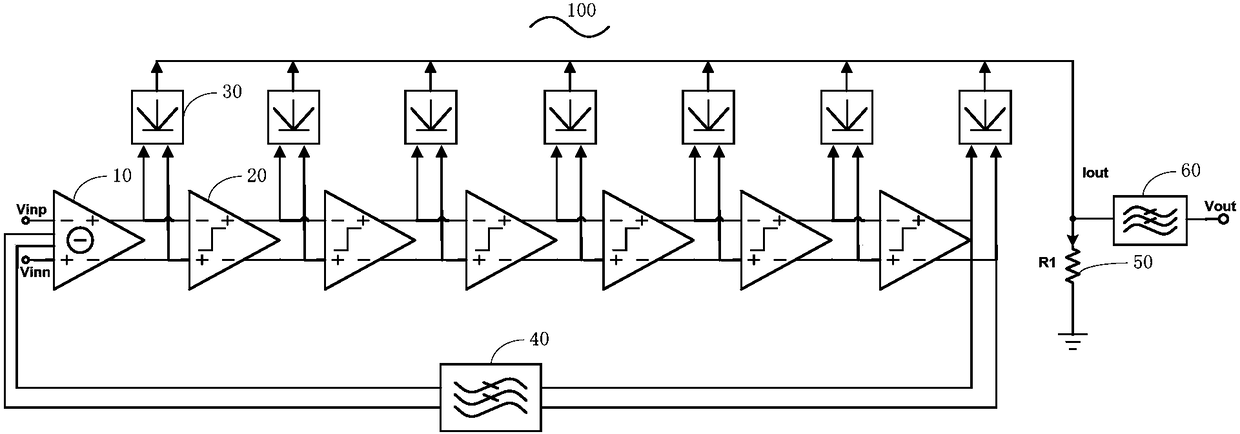
[0070] Such as figure 1 As shown, this embodiment provides a power detection circuit 100, which includes an offset subtractor 10, several limiting amplifiers 20, several rectifiers 30, an active low-pass filter 40, an impedance device 50 and a passive low-pass filter 60 .

[0071] In specific applications, any type of limiting amplifier, rectifier, impedance device and passive low-pass filter can be selected according to actual needs. For example, resistance devices can be selected as impedance devices.

[0072] In this embodiment, the impedance device 50 is a resistance device, figure 1 Expressed as the resistor R1.

[0073] In specific applications, the number of limiting amplifiers 20 and rectifiers 30 can be selected according to actual needs, and the number of rectifiers is equal to the sum of the number of limiting amplifiers and the number of offset subtractors. The number of cascaded limiting amplifiers is related to the linear detection range of the power detection...

Embodiment 2

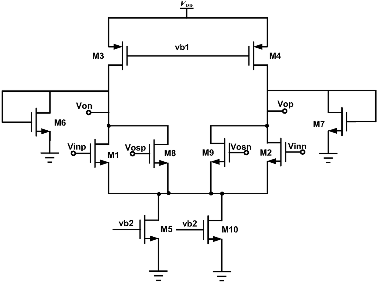
[0087] Such as figure 2 As shown, in this embodiment, the offset subtractor 10 in the first embodiment includes first to tenth field effect transistors, denoted as M1 to M10 respectively;

[0088] Wherein, the first to eighth field effect transistors M1 to M8 are N-type field effect transistors, and the ninth and tenth field effect transistors M9 and M10 are P-type field effect transistors.

[0089] Such as figure 2 As shown, the connection relationship between the devices in the offset subtractor 10 provided by this embodiment is as follows:

[0090] The gate of the first field effect transistor M1 is the negative input terminal Vinp of the offset subtractor 10, the source of the first field effect transistor M1 is connected to the source of the second field effect transistor M2, the drain of the fifth field effect transistor M5, and the second field effect transistor M5. The source of the eighth field effect transistor M8, the source of the ninth field effect transistor ...

Embodiment 3

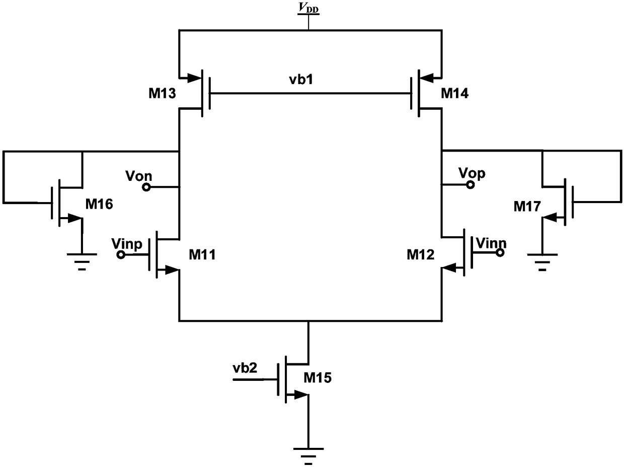
[0101] Such as image 3 As shown, in this embodiment, the limiting amplifier 20 in the first embodiment includes eleventh to seventeenth field effect transistors, denoted as M11 to M17 respectively; wherein, the eleventh field effect transistor M11, the twelfth field effect transistor The field effect transistor M12 and the fifteenth to seventeenth field effect transistors M15 to M17 are N-type field effect transistors, and the thirteenth field effect transistor M13 and the fourteenth field effect transistor M14 are P-type field effect transistors.

[0102] Such as image 3 As shown, the connection relationship between each device in the limiting amplifier 20 provided by this embodiment is as follows:

[0103] The gate of the eleventh field effect transistor M11 is the inverting input terminal Vinp of the limiting amplifier 20, the source of the eleventh field effect transistor M11 is connected to the source of the twelfth field effect transistor M12 and the fifteenth field e...


PUM


Abstract

The invention is applicable to the technical field of communication, and provides a power detection circuit. The power detection circuit comprises offset subtractors, a plurality of limiting amplifiers, a plurality of rectifiers, an active low-pass filter, an impedance device and a passive low-pass filter, wherein a detection signal is input in the first input end of the offset subtractor, the offset subtractors and the plurality of limiting amplifiers are cascaded in sequence, the output end of the offset subtractor and the output end of each level of limiting amplifier are correspondingly connected with an input end of one rectifier separately, the output end of the last level of limiting amplifier is connected with the input end of the active low-pass filter, the output ends of the plurality of rectifiers are connected in sequence and then are connected with both the input end of the impedance device and the input end of the passive low-pass filter, the output end of the active low-pass filter is connected with the second input end of the offset subtractor, and the output end of the impedance device is grounded. The power detection circuit can rapidly eliminate direct current offset of a detection signal of low frequency, and can reduce the layout area remarkably.

Description

technical field [0001] The invention belongs to the technical field of communication, and in particular relates to a power detection circuit. Background technique [0002] With the rapid development of modern communication technology, the market audience of the communication industry continues to expand, and communication systems are widely used. As the basic module of the communication system, the radio frequency receiver has also been widely used, and the performance improvement and potential exploration of the radio frequency receiver have become a research hotspot in the field of communication technology. [0003] As the working environment of the radio frequency receiver changes, the effective signal power received by its antenna will change within a possible range, and the interference power received by the antenna may also change. In order to correctly demodulate the signal received by the antenna, the automatic gain control system needs to adjust the gain to maintai...

Claims


Application Information

Patent Timeline
Patent Type & Authority Applications(China)
IPC IPC(8): H03H7/01H04B17/29
CPCH03H7/0161H04B17/29
Inventor 章松曾隆月
Owner SHENZHEN JOINTWAY IC DESIGN CO LTD
Why Eureka
Try Eureka