Composite channel transistor and preparation method thereof

A composite channel and transistor technology, applied in semiconductor/solid-state device manufacturing, electric solid-state devices, semiconductor devices, etc., can solve problems such as unsatisfactory conductivity and low mobility, and achieve convenient preparation and simple and feasible preparation process Effect

Active Publication Date: 2018-08-07
SHANGHAI INTEGRATED CIRCUIT RES & DEV CENT
View PDF4 Cites 1 Cited by
  • Summary
  • Abstract
  • Description
  • Claims
  • Application Information

AI Technical Summary

Problems solved by technology

[0008] However, most organic materials are n

Method used


Image

  • Composite channel transistor and preparation method thereof
  • Composite channel transistor and preparation method thereof
  • Composite channel transistor and preparation method thereof

Examples


Embodiment Construction

[0040] The specific embodiments of the present invention will be further described in detail below with reference to the accompanying drawings.

[0041] It should be noted that in the following specific embodiments, when the embodiments of the present invention are described in detail, in order to clearly show the structure of the present invention for ease of description, the structure in the drawings is not drawn according to the general scale. Partial enlargement, deformation, and simplification of processing have been implemented. Therefore, this should be avoided as a limitation of the present invention.

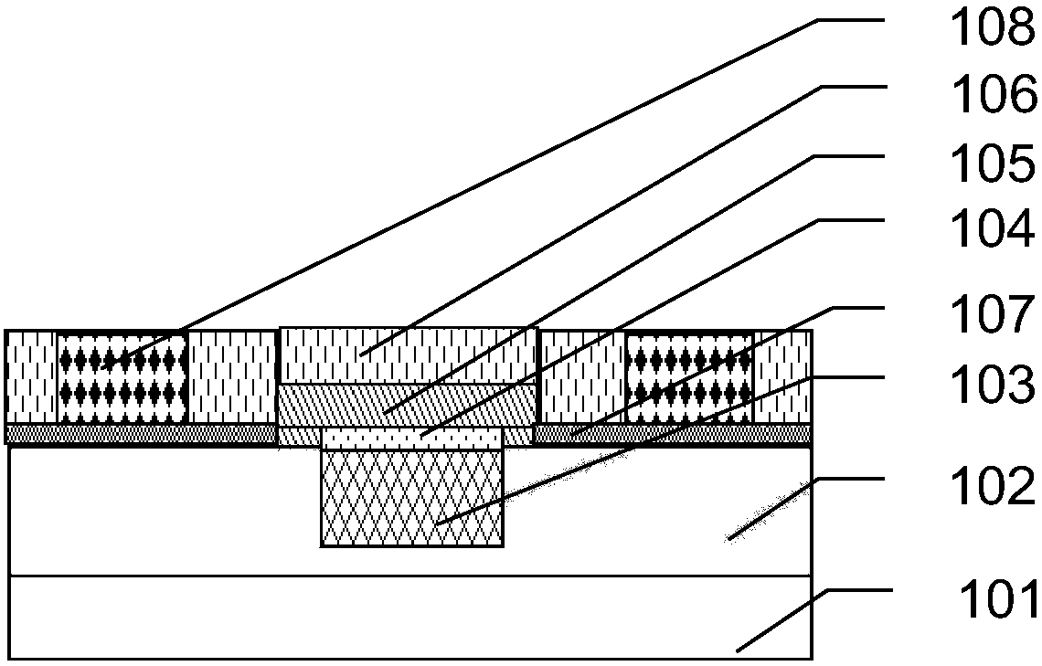
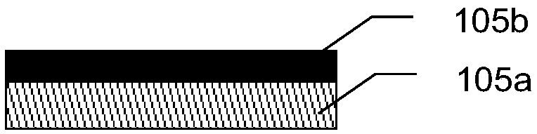
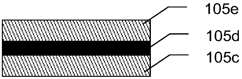
[0042] In the following specific embodiments of the present invention, please refer to figure 1 , figure 1 It is a schematic diagram of a composite channel transistor structure according to a preferred embodiment of the present invention. Such as figure 1 As shown, a composite channel transistor of the present invention includes at least a semiconductor substrate 101, an int...


PUM


Abstract

The invention discloses a composite channel transistor comprising the following parts: an interlayer dielectric layer formed on a semiconductor substrate; a grid electrode formed in the interlayer dielectric layer; a grid dielectric layer arranged on the grid electrode; a composite channel layer located on the grid dielectric layer and the interlayer dielectric layer; source drain zones formed ontwo ends of the composite channel layer; a passivation layer formed on the interlayer dielectric layer and that wraps the periphery and top surface of the composite channel layer; source-drain electrodes arranged in the passivation layer and connected with the source drain zones. The method uses a high mobility graphene and an organic film with adjustable band gaps to commonly form the composite channel layer, thus effectively solving the problems that the graphene has no band gap and the organic film transistor is low in mobility; the method can prepare the composite channel transistor with ahigh mobility, is compatible with existing CMOS process, simple and feasible in preparation process, and can easily prepare a composite channel transistor array with a small size and a large scale; the invention also discloses the composite channel transistor preparation method.

Description

Technical field [0001] The present invention relates to the technical field of semiconductor integrated circuit manufacturing, and more specifically, to a composite channel transistor and a preparation method thereof. Background technique [0002] As the feature size of semiconductor devices shrinks in proportion, the chip integration degree continues to increase. Due to process limitations and various negative effects, traditional silicon-based semiconductor devices can no longer meet the performance and power consumption requirements of devices and circuits. Major domestic and foreign scientific research institutions and semiconductor manufacturers have studied various new materials and new device structures in order to replace the existing silicon semiconductor devices. [0003] In recent years, graphene due to its ultra-high electron mobility (up to 200,000 cm 2 / Vs) has become a research hotspot, but because graphene does not have a bandgap, its prospects for applications simi...

Claims


Application Information

Patent Timeline
IPC IPC(8): H01L51/05H01L51/40
CPCH10K10/488
Inventor 钟旻陈寿面
Owner SHANGHAI INTEGRATED CIRCUIT RES & DEV CENT
Why Eureka
Try Eureka