
Manufacturing method of semiconductor element and manufacturing method of solar cell

A manufacturing method and semiconductor technology, which are applied in the fields of semiconductor/solid-state device manufacturing, semiconductor devices, electrical components, etc., can solve the problem of increasing the number of steps, and achieve the effect of reducing the number of steps and suppressing out-diffusion.

Active Publication Date: 2022-05-17
TORAY IND INC
View PDF10 Cites 0 Cited by
  • Summary
  • Abstract
  • Description
  • Claims
  • Application Information

AI Technical Summary

Problems solved by technology

However, in such a method, there is a problem that the number of steps increases

Method used


Image

  • Manufacturing method of semiconductor element and manufacturing method of solar cell
  • Manufacturing method of semiconductor element and manufacturing method of solar cell
  • Manufacturing method of semiconductor element and manufacturing method of solar cell

Examples


Embodiment 1

[0121] Into a 500mL three-necked flask, 20.8g of polyvinyl alcohol (manufactured by Wako Pure Chemical Industries, the degree of polymerization is 500) and 144g of water were dropped into, and the temperature was raised to 80°C while stirring, and after stirring for 1 hour, propylene glycol monomethyl ether ( KH Neochem Co., Ltd.) 231.6 g and 3.6 g of diboron trioxide were stirred at 80° C. for 1 hour. After cooling to 40° C., 0.12 g of a fluorine-based surfactant MEGAFACE F477 (manufactured by DIC Corporation) was added and stirred for 30 minutes to prepare a p-type impurity diffusion composition.

[0122] Next, on one surface of the n-type semiconductor substrate textured on both surfaces, the p-type impurity diffusion composition was coated on the entire surface by spin coating, and dried at 150° C. for 1 minute to produce a pattern formed on one surface. A semiconductor substrate having a p-type impurity diffusion composition film.

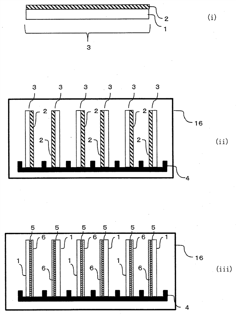
[0123] Next, if figure 1 As shown in ...

Embodiment 2

[0130] On one surface of an n-type semiconductor substrate textured on both surfaces, the same p-type impurity diffusion composition as in Example 1 was coated on the entire surface by spin coating, and dried at 150° C. for 1 minute to fabricate A semiconductor substrate having a p-type impurity diffusion composition film formed on one surface.

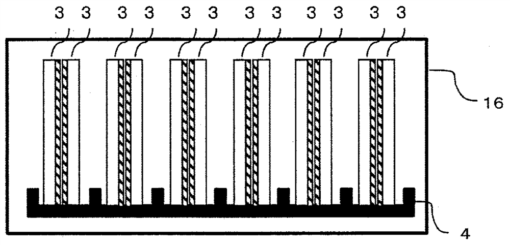
[0131] Next, if figure 2 As shown, a semiconductor substrate having a p-type impurity diffusion composition film formed on one surface is disposed on the diffusion plate. The distance between the surfaces on which the p-type impurity-diffusion composition film was formed was 0 mm, and the distance between the surfaces on which the p-type impurity-diffusion composition film was not formed was 3 mm in a pair of semiconductor substrates.

[0132] Next, in circulation O 2 : 0.2L / min, N 2 : In a 9.8 L / min diffusion furnace (Koyo Thermo Systems Co., Ltd., 206A-M100), a diffusion plate was placed in a state set at 700°C. Thereafter, the...

Embodiment 3

[0138] On one surface of an n-type semiconductor substrate textured on both surfaces, the same p-type impurity diffusion composition as in Example 1 was coated on the entire surface by spin coating, and dried at 150° C. for 1 minute to fabricate A semiconductor substrate having a p-type impurity diffusion composition film formed on one surface.

[0139] Next, if figure 2As shown, a semiconductor substrate having a p-type impurity diffusion composition film formed on one surface is disposed on the diffusion plate. The distance between the surfaces on which the p-type impurity-diffusion composition film was formed was 0 mm, and the distance between the surfaces on which the p-type impurity-diffusion composition film was not formed was 3 mm in a pair of semiconductor substrates.

[0140] Next, in circulation O 2 : 0.2L / min, N 2 : In a 9.8 L / min diffusion furnace (Koyo Thermo Systems Co., Ltd., 206A-M100), a diffusion plate was placed in a state set at 700°C. Thereafter, the ...


PUM

PropertyMeasurementUnit
thicknessaaaaaaaaaa

Abstract

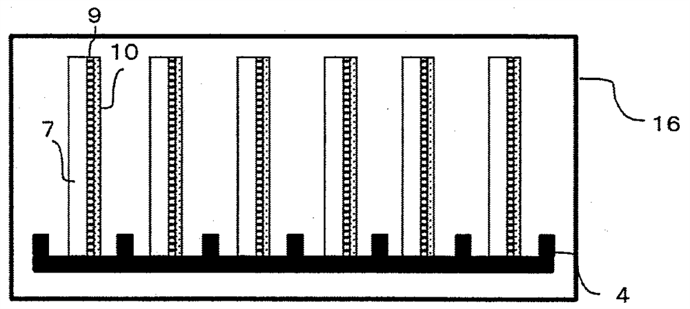
A method of manufacturing a semiconductor element, which is a method of manufacturing a semiconductor element using a plurality of semiconductor substrates, characterized in that it includes the following steps (a) to (c), and in the steps (b) and (c), the A set of two semiconductor substrates is arranged such that the surfaces on which the impurity diffusion composition film of the first conductivity type is formed face each other, (a) one surface of each semiconductor substrate is coated with the impurity of the first conductivity type The step of diffusing the composition to form a film of the impurity-diffusing composition of the first conductivity type; (b) heating the semiconductor substrate on which the film of the impurity-diffusing composition of the first conductivity type is formed so that the impurities of the first conductivity type A step of diffusing the aforementioned semiconductor substrate to form a first conductivity type impurity diffusion layer; (c) heating the aforementioned semiconductor substrate in an atmosphere containing a second conductivity type impurity to cause the second conductivity type impurity to the aforementioned A step in which the other surface of the semiconductor substrate is diffused to form an impurity diffusion layer of the second conductivity type. Provided is a semiconductor element and a solar cell manufacturing method capable of efficiently manufacturing the semiconductor element and solar cell by reducing the number of steps.

Description

technical field [0001] The invention relates to a method of manufacturing a semiconductor-based element and a method of manufacturing a solar cell. Background technique [0002] Among conventional solar cells, a double-side light-receiving type solar cell capable of receiving light from both sides is known. Two-sided light-receiving solar cells have been proposed that are installed on a wall or the like to receive light on both sides, and those that have a back sheet having a reflective function on the back side and are installed on a structure such as a roof to receive light on both sides. (For example, refer to Patent Document 1). [0003] In a semiconductor substrate used in a solar cell, in order to diffuse p-type and n-type impurities to form an impurity diffusion layer, a method of forming a p-type impurity diffusion layer and an n-type impurity diffusion layer in separate steps is used. However, such a method has a problem of increasing the number of steps. [0004...

Claims


Application Information

Patent Timeline
Patent Type & Authority Patents(China)
IPC IPC(8): H01L21/22H01L31/068H01L31/18H01L21/225H01L21/223
CPCH01L21/22H01L21/223H01L21/225H01L31/068H01L31/18Y02E10/547Y02P70/50
Inventor 池上由洋稻叶智雄
Owner TORAY IND INC
Learn More