

Method for improving uniformity of doping concentration of silicon epitaxial layer for photosensor
A photoelectric sensor and doping concentration technology, which is applied in the direction of circuits, electrical components, semiconductor devices, etc., can solve the problems of poor consistency and achieve the effect of improving the consistency of distribution
- Summary
- Abstract
- Description
- Claims
- Application Information
AI Technical Summary
Problems solved by technology
Method used
Image

Examples
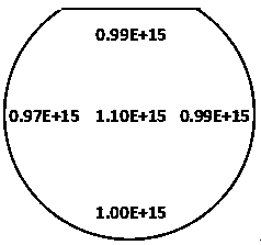
Embodiment 1
[0028] In the first step, hydrogen gas is introduced into the reaction chamber, and the flow rate of hydrogen gas is set to 20 L / min. Then, hydrogen chloride gas is introduced, and the flow rate of hydrogen chloride gas is set to 30 L / min. etched, the reaction temperature was set at 1080°C, and the reaction time was set at 5 min; in the second step, the flow rate of hydrogen gas was set at 150 L / min, gaseous trichlorosilane was introduced, and the flow rate was set at 6 L / min, and the deposition The time was set at 2 min, and the surface of the epitaxial reaction base was covered with a layer of undoped polysilicon.
[0029] The third step is to install the silicon substrate on the polysilicon layer on the epitaxial reaction base, and use nitrogen and hydrogen to purge the epitaxial reaction chamber in sequence. The flow rate of nitrogen gas is set to 100 L / min, and the flow rate of hydrogen gas is set to 150 L / min. L / min, the chamber purge time was set to 10 min.
[0030] Th...
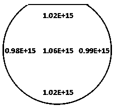
Embodiment 2
[0037]In the first step, hydrogen gas is introduced into the reaction chamber, and the flow rate of hydrogen gas is set to 20 L / min. Then, hydrogen chloride gas is introduced, and the flow rate of hydrogen chloride gas is set to 30 L / min. Corrosion, the reaction temperature was set at 1080 °C, and the reaction time was set at 5 min;
[0038] In the second step, set the flow rate of hydrogen to 150 L / min, pass through gaseous trichlorosilane, set the flow rate to 6 L / min, set the deposition time to 2 min, and cover the surface of the base with a layer of undoped Polysilicon;
[0039] The third step is to install the silicon substrate on the polysilicon on the epitaxial reaction base, and then use nitrogen and hydrogen to purge the epitaxial reaction chamber in sequence. The flow rate of nitrogen gas is set to 100 L / min, and the flow rate of hydrogen gas is set to 150 L / min, the chamber purge time is set to 10 min.
[0040] The fourth step is to heat the epitaxial reaction ba...
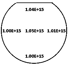
Embodiment 3
[0048] In the first step, hydrogen gas is introduced into the reaction chamber, and the flow rate of hydrogen gas is set to 20 L / min. Then, hydrogen chloride gas is introduced, and the flow rate of hydrogen chloride gas is set to 30 L / min. etched, the reaction temperature was set at 1080 °C, and the reaction time was set at 5 min.
[0049] In the second step, set the flow rate of hydrogen to 150 L / min, feed gaseous trichlorosilane, set the flow rate to 6 L / min, set the deposition time to 2 min, and cover the surface of the epitaxial reaction base with a layer of non-doped Miscellaneous polysilicon.
[0050] The third step is to install the silicon substrate on the polysilicon on the epitaxial reaction base, and then use nitrogen and hydrogen to purge the epitaxial reaction chamber in sequence. The flow rate of nitrogen gas is set to 100 L / min, and the flow rate of hydrogen gas is set to 150 L / min, the chamber purge time is set to 10 min.
[0051] The fourth step is to heat ...
PUM
 Abstract
Description
Claims
Application Information