A method for improving the uniformity of doping concentration of silicon epitaxial layer for photoelectric sensors

A photoelectric sensor and doping concentration technology, which is applied in the direction of circuits, electrical components, semiconductor devices, etc., can solve the problems of poor consistency and achieve the effect of improving the consistency of distribution

Active Publication Date: 2020-05-12
CHINA ELECTRONICS TECH GRP NO 46 RES INST
View PDF8 Cites 0 Cited by
  • Summary
  • Abstract
  • Description
  • Claims
  • Application Information

AI Technical Summary

Problems solved by technology

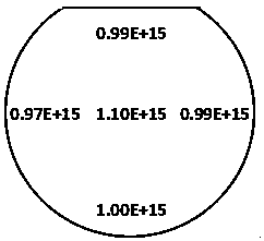
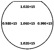
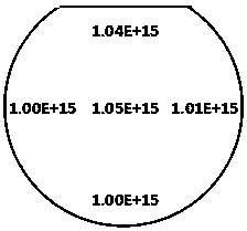
[0003] The purpose of the present invention is to overcome the problem that the doping concentration of the P-type silicon epitaxial layer used in the existing photoelectric sensor is affected by self-doping in the chip and between the chips, and the consistency is poor. By implementing the main process before the growth of the doped epitaxial layer The rapid change of the gas flow rate and the two intrinsic layer growth processes sweep most of the impurities volatilized at high temperature out of the cavity, reducing the influence of substrate impurities on the self-doping during the growth of the epitaxial layer, and obtaining a A preparation method for improving the uniformity of doping concentration of silicon epitaxial layer for photoelectric sensors

Method used


Image

  • A method for improving the uniformity of doping concentration of silicon epitaxial layer for photoelectric sensors
  • A method for improving the uniformity of doping concentration of silicon epitaxial layer for photoelectric sensors
  • A method for improving the uniformity of doping concentration of silicon epitaxial layer for photoelectric sensors

Examples


Embodiment 1

[0028] The first step is to pass hydrogen into the reaction chamber. The hydrogen flow rate is set to 20L / min, and then the hydrogen chloride gas is passed into it. The hydrogen chloride gas flow rate is set to 30L / min, and the residual deposits on the epitaxial reaction base are engraved at high temperature. For corrosion, the reaction temperature is set to 1080 ℃, the reaction time is set to 5 min; the second step, the hydrogen flow is set to 150L / min, the gaseous trichlorosilane is introduced, the flow is set to 6 L / min, and the deposition The time is set to 2 min, and the surface of the epitaxial reaction base is covered with a layer of undoped polysilicon.

[0029] In the third step, the silicon substrate is loaded on the polysilicon layer on the epitaxial reaction base, and the epitaxial reaction chamber is purged with nitrogen and hydrogen in sequence. The flow of nitrogen is set to 100 L / min, and the flow of hydrogen is set to 150 L / min, the cavity purge time is set to 10...

Embodiment 2

[0037] The first step is to pass hydrogen into the reaction chamber. The hydrogen flow rate is set to 20L / min, and then the hydrogen chloride gas is passed into it. The hydrogen chloride gas flow rate is set to 30L / min, and the residual deposits on the epitaxial reaction base are engraved at high temperature. For corrosion, the reaction temperature is set to 1080℃, and the reaction time is set to 5 min;

[0038] The second step is to set the hydrogen flow rate to 150L / min, pass in the gaseous trichlorosilane, set the flow rate to 6 L / min, set the deposition time to 2 min, and cover the surface of the base with a layer of undoped Polysilicon

[0039] The third step is to load the silicon substrate on the polysilicon on the epitaxial reaction pedestal, and purge the epitaxial reaction chamber with nitrogen and hydrogen in sequence. The flow of nitrogen is set to 100 L / min, and the flow of hydrogen is set to 150 L / min, the cavity purge time is set to 10 min.

[0040] The fourth step ...

Embodiment 3

[0048] The first step is to pass hydrogen into the reaction chamber. The hydrogen flow rate is set to 20L / min, and then the hydrogen chloride gas is passed into it. The hydrogen chloride gas flow rate is set to 30L / min, and the residual deposits on the epitaxial reaction base are engraved at high temperature. For corrosion, the reaction temperature is set to 1080 ℃, and the reaction time is set to 5 min.

[0049] The second step is to set the hydrogen flow rate to 150L / min, pass in the gaseous trichlorosilane, set the flow rate to 6 L / min, set the deposition time to 2 min, and cover the surface of the epitaxial reaction base with no doped Miscellaneous polysilicon.

[0050] The third step is to load the silicon substrate on the polysilicon on the epitaxial reaction pedestal, and purge the epitaxial reaction chamber with nitrogen and hydrogen in sequence. The flow of nitrogen is set to 100 L / min, and the flow of hydrogen is set to 150 L / min, the cavity purge time is set to 10 min....


PUM

PropertyMeasurementUnit
diameteraaaaaaaaaa
thicknessaaaaaaaaaa

Abstract

The invention relates to a method for improving the uniformity of doping concentration of a silicon epitaxial layer for a photosensor. The method includes the steps of introducing hydrogen and hydrogen chloride gas into a reaction chamber; coating the surface of an epitaxial reaction substrate with an undoped polysilicon layer; loading a silicon base sheet onto the polysilicon, and purging the epitaxial reaction chamber sequentially with nitrogen and hydrogen; heating the epitaxial reaction substrate; introducing hydrogen chloride gas to polish the surface of the silicon base sheet; purging the reaction chamber by quick periodic alternating variation of flow; growing a first intrinsic epitaxial layer; introducing hydrogen into the reaction chamber for purging; growing a second intrinsic epitaxial layer; purging the reaction chamber by quick periodic alternating variation of flow; growing a doped epitaxial layer; and after the growth of the epitaxial layer is completed, stopping heating, and finally taking out the chip. The beneficial effect is that the on-chip non-uniformity is reduced from 5.09% to the level of 1.48%, the control capability is improved, and the process capabilitycan meet the requirements of users.

Description

Technical field [0001] The invention relates to the technical field of preparation of semiconductor epitaxial materials, in particular to a method for improving the uniformity of doping concentration of a silicon epitaxial layer for a photoelectric sensor. Background technique [0002] The current trend of high-speed development of photoelectric sensors represented by CCD devices with high sensitivity, high resolution, and wide dynamic range requires that the doping concentration of the P-type silicon epitaxial layer, which is the key support material, be highly consistent to meet The working voltage, sensitivity and other index requirements of the device. However, since the growth of the silicon epitaxial layer is based on a heavily doped boron impurity substrate, boron atoms have the characteristics of light weight, long free path, and extremely volatile. Under the epitaxial reaction temperature higher than 1000 ℃, the volatilization effect of substrate impurities continues to ...

Claims


Application Information

Patent Timeline
Patent Type & Authority Patents(China)
IPC IPC(8): H01L21/02H01L31/0288H01L31/101
CPCH01L21/02532H01L21/02595H01L21/02634H01L31/0288H01L31/101
Inventor 李明达周幸李杨
Owner CHINA ELECTRONICS TECH GRP NO 46 RES INST
Why Eureka
Try Eureka